Method for fabricating transistor of semiconductor device

Inactive Publication Date: 2005-08-30
DONGBUANAM SEMICON
View PDF8 Cites 9 Cited by
  • Summary
  • Abstract
  • Description
  • Claims
  • Application Information

AI Technical Summary

Benefits of technology

[0019]In forming the sacrificial layer, length of the sacrificial layer can be adjusted appropriately and, therefore, length of the remaining sacrificial layer on the substrate, which forms two spacers, can be adjusted. Such adjustment of length can prevent the effective channel length from being shortened. In addition, the present inv

Problems solved by technology

However, the above-mentioned conventional methods of fabricating a transistor can cause the following problems.
Second, when an ion implantation is performed to form the source/drain region, out-diffusion of ions, whic

Method used


Image

  • Method for fabricating transistor of semiconductor device
  • Method for fabricating transistor of semiconductor device
  • Method for fabricating transistor of semiconductor device

Examples


Embodiment Construction

[0024]Reference will now be made in detail to the preferred embodiments of the present invention, examples of which are illustrated in the accompanying drawings.

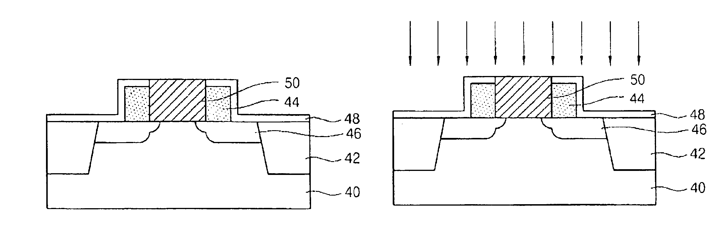
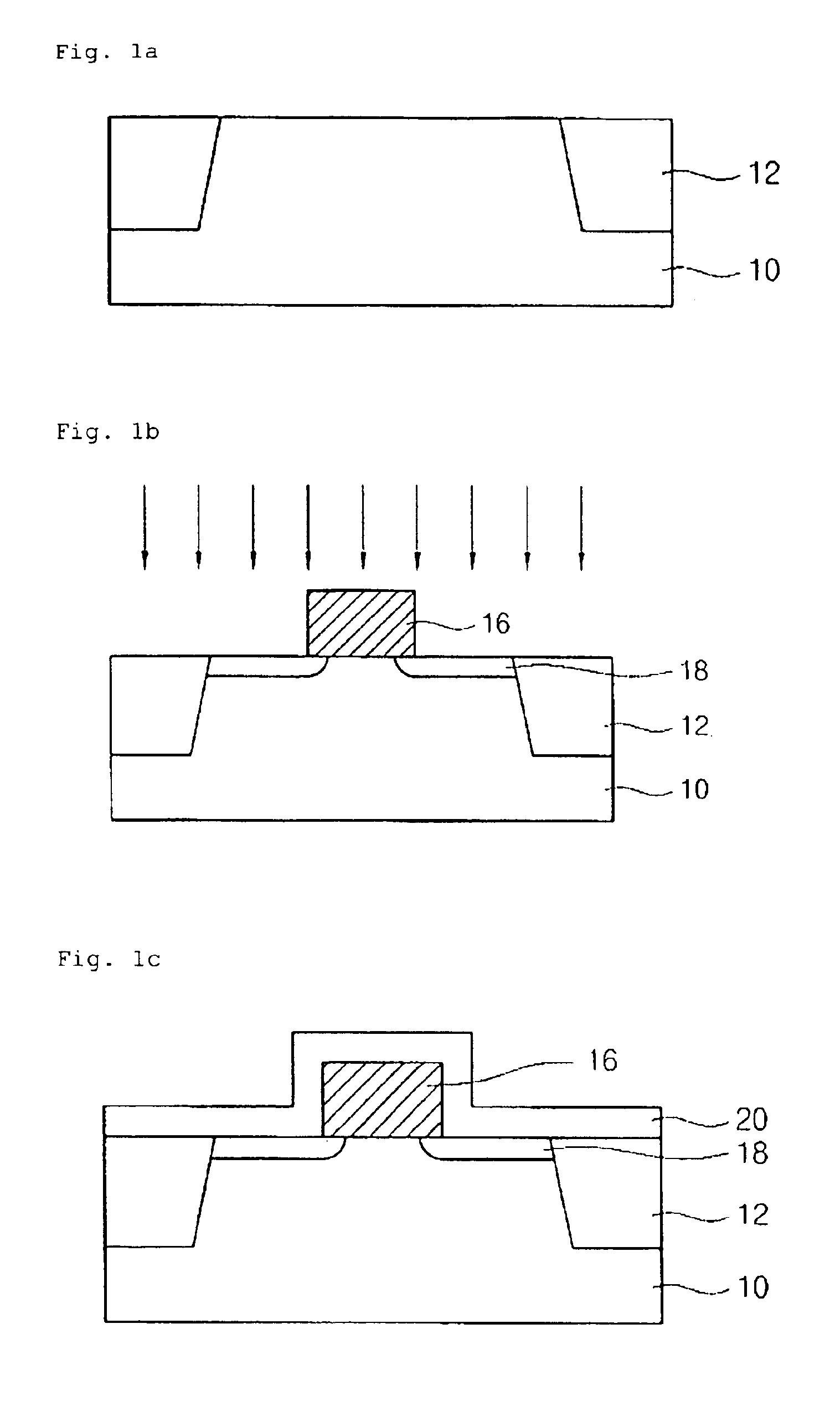
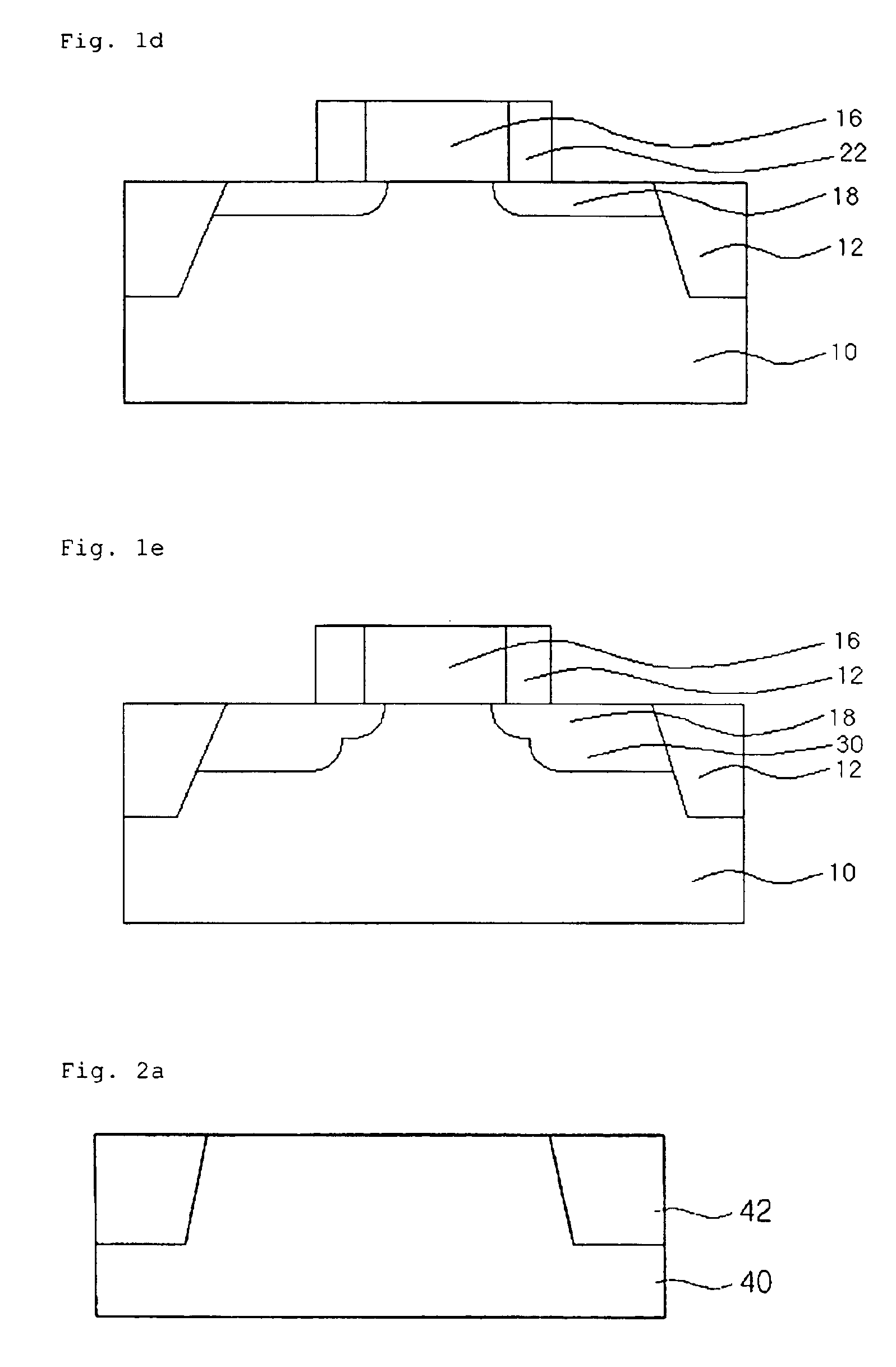
[0025]Referring to FIG. 2a, a substrate 40 with device isolation layers 42 is provided. The device isolation layers 42 preferably have a trench structure. The trench structure has an advantage that it has a smaller area than a field oxide.

[0026]Referring to FIG. 2b, a sacrificial layer 44 is formed on the substrate 40. The sacrificial layer 44 is preferably made of silicon oxide or silicon nitride. In addition, the sacrificial layer 44 is formed only on an active region of the substrate 40 by means of patterning. In detail, a thin layer of sacrificial material is deposited on the substrate and some part of the thin layer is removed to form the sacrificial layer 44. Here, length of the sacrificial layer is appropriately adjusted so that length of two spacers to be formed later can be adjusted to prevent the effective channel ...


PUM


Abstract

A method of fabricating a transistor of a semiconductor device is disclosed. The method of fabricating a transistor comprises forming a sacrificial layer on a substrate; forming a source/drain region in the substrate by performing a first ion implantation using the sacrificial layer as a mask; forming a barrier layer over the substrate with the sacrificial layer; removing a portion of the sacrificial layer to form an opening through which a portion of the substrate is exposed; performing a second ion implantation using the opening as a mask to implant ions for adjustment of a threshold voltage of the substrate; forming a gate electrode on the substrate exposed through the opening; and performing a third ion implantation to adjust doping concentration in the gate electrode. Accordingly, the present invention can reduce the occurrences of a short channel effect and a reverse short channel effect in a transistor.

Description

BACKGROUND OF THE INVENTION[0001]1. Field of the Invention[0002]The present invention relates to a method for fabricating a semiconductor device and, more particularly, to a method for fabricating a transistor of a semiconductor device.[0003]2. Background of the Related Art[0004]Most semiconductor devices comprise transistors. FIGS. 1a through 1e illustrate, in cross-sectional views, the process steps for forming a transistor in a semiconductor device according to a conventional art. Referring to FIG. 1a, a substrate 10 with device isolation layers 12 is provided and an ion implantation is performed on the substrate 10 in order to adjust a threshold voltage. Referring to FIG. 1b, a gate electrode 16 is formed on the substrate 10. Then, a first source / drain region 18 with shallow junction is formed in the substrate 10 by performing an ion implantation using the gate electrode 16 as a mask. Referring to FIGS. 1c and 1d, an insulating layer 20 is deposited over the substrate 10 with th...

Claims


Application Information

Patent Timeline
IPC IPC(8): H01L21/02H01L21/336H01L29/78
CPCH01L29/66568H01L29/66537H01L29/78
Inventor CHOI, CHEE HONGKIM, TAE WOO
Owner DONGBUANAM SEMICON
Why Eureka
Try Eureka