Photoelectric conversion device and solid-state image sensing device using the same

a conversion device and solid-state image technology, applied in the direction of material analysis, radiation control devices, instruments, etc., can solve the problems of large number of defects produced at the interface, dark current, etc., to prevent electrons, facilitate the planarization of the substrate surface, and prevent the peeling off of the injection inhibiting layer

Inactive Publication Date: 2005-08-30
MINOLTA CO LTD
View PDF12 Cites 14 Cited by
  • Summary
  • Abstract
  • Description
  • Claims
  • Application Information

AI Technical Summary

Benefits of technology

[0013]On the other hand, the composition ratio N/Si of the hole injection inhibiting layer, i.e., the amorphous silicon nitride layer of the n-type conductivity may be adjusted appropriately to 0.8 or lower. When the composition ratio is within the range, it is possible to provide the energy level at the interface between the amorphous silicon nitride layer and the amorphous silicon layer which is discontinued only on the valence band side and equal on the conduction band side. In other words, it is possible to prevent electrons from flowing out of the carrier generation/multiplication layer, while preventing injection of holes into the carrier generation/multiplication layer. As a result, electrons as the other type of carriers can be retrieved, while a dark current is suppressed.
[0014]The aforesaid layered structure may be formed appropriately on a surface of a substrate having at least the surface composed of polycrystalline silicon or microcrystalline silicon. The layered structure may also be formed on a surface of a substrate having at least the surface composed of monocrystalline silicon. It follows that the amorphous silicon carbide layer as the electron injection inhibiting layer or the amorphous silicon nitride layer as the hole injection inhibiting layer is formed on a silicon-based material having a thermal expansion coefficient close to that of the injection inhibiting layer. This prevents the peeling off of the injection inhibiting layer due to thermal expansion. This also facilitates planarization of a substrate surface and formation of the layers with equal thicknesses, so that an electric field is applied uniformly to the entire light-receiving surface of the carrier generation/multiplication layer. As a result, the electric field is prevented from being localized so that the efficiency of photoelectric conversion is equal at any portion of the carrier generation/multiplication layer.
[0015]The layered structure can also be formed on a surface of a substrate having at least the surface composed of a metal. This significantly facilitates planarization of a substrate surface...

Problems solved by technology

However, since the carrier generation layer and the carrier multiplication layer exist separately in the reach-through structure, it assumes a complicated structure consisting of a large number of layers so that interfaces between the layers are increase...

Method used


Image

  • Photoelectric conversion device and solid-state image sensing device using the same
  • Photoelectric conversion device and solid-state image sensing device using the same
  • Photoelectric conversion device and solid-state image sensing device using the same

Examples


first embodiment

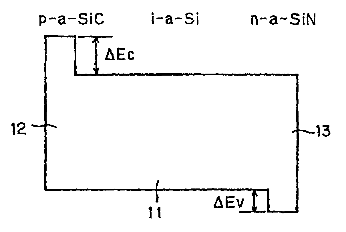
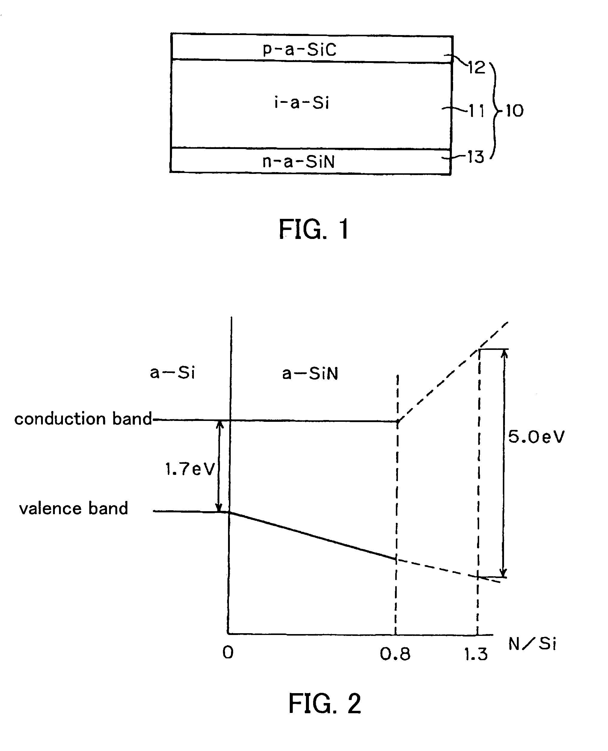
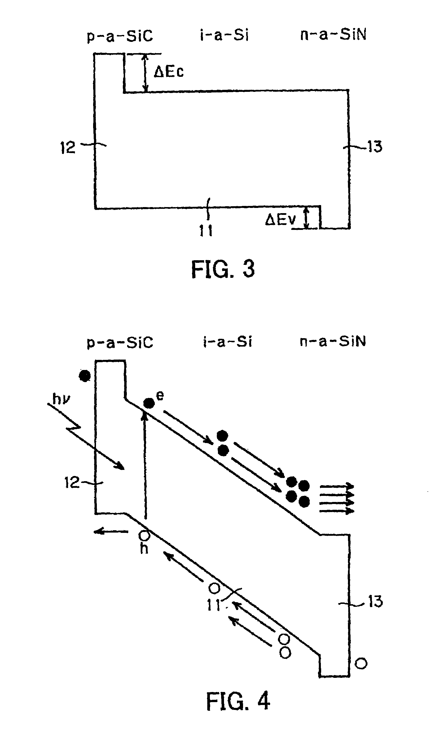
[0047]A cross section of a photoelectric conversion device 1 of the first embodiment is shown diagrammatically in FIG. 5. The photoelectric conversion device 1 is obtained by forming the three-layered structure 10 on a substrate 21 made of monocrystalline silicon. The silicon substrate 21 is of n-type and the n-a-SiN hole injection inhibiting layer 13 is in contact with the silicon substrate 21. A transparent electrode 22 made of gold (Au) is provided on the p-a-SiC electron injection inhibiting layer 12.

[0048]The following is a specific example of a method of fabricating the photoelectric conversion device 1. First, the n-type silicon substrate 21 is placed in a deposition chamber of a capacitively-coupled parallel-plate plasma CVD system and heated by a heater such that the temperature of the substrate 21 is increased to 250° C. Then, the deposition chamber is sufficiently vacuumed so that a silane gas diluted to 10% with hydrogen, an ammonia gas diluted to 10% with hydrogen, and ...

second embodiment

[0055]A cross section of a photoelectric conversion device 2 of a second embodiment is shown diagrammatically in FIG. 7. The photoelectric current conversion device 2 is formed by using a p-type monocrystalline silicon for a substrate 23 such that the p-a-SiC electron injection inhibiting layer 12 is in contact with the silicon substrate 23. A transparent electrode 24 made of ITO is provided on the n-a-SiN hole injection inhibiting layer 13.

[0056]The photoelectric conversion device 2 is fabricated by forming the electron injection inhibiting layer 12, the carrier generation / multiplication layer 11, the hole injection inhibiting layer 13, and the transparent electrode 24 in this order. Since only the order in which the layers are formed is different and the processes in the individual steps are the same as described in the example of the fabrication of the photoelectric conversion device 1, the overlapping description will be omitted.

[0057]The photoelectric conversion device 2 of the...

third embodiment

[0058]A cross section of a solid-state image sensing device 3 of a third embodiment is shown diagrammatically in FIG. 8. The solid-state image sensing device 3 is of CCD type and has the three-layered structure 10 as a photoelectric conversion unit provided on a multilayer structure. FIG. 8 indicates a range containing one pixel in the solid-state image sensing device 3.

[0059]The following is a specific example of a method of fabricating the solid-state image sensing device 3. First, a p+-type device isolation region 32 is provided in the p-type silicon substrate 31 and an accumulation diode 33 composed of an n+-type impurity region is formed in the area surrounded by the p+-type device isolation region 32. An n-type channel region 34 of a vertical CCD is provided adjacent the accumulation diode 33. Subsequently, a first insulating film 35 is formed of a silicon oxide film over the entire top surface of the substrate 31. During the formation of the insulating film 35, transfer gate ...


PUM


Abstract

Disclosed is a photoelectric conversion device having a multiplying function and an image sensing device using the same. The photoelectric conversion device essentially comprises three layered structure: a carrier generation/multiplication layer composed of amorphous silicon to have both the function of absorbing light and generating carriers through optical excitation and the function of multiplying the generated carriers; an electron injection inhibiting layer composed of an amorphous silicon carbide of the p-type conductivity to inhibit injection of electrons into the carrier generation/multiplication layer; and a hole injection inhibiting layer composed of an amorphous silicon nitride of the n-type conductivity to inhibit injection of holes into the carrier generation/multiplication layer. The said carrier generation/multiplication layer is provided between said electron injection inhibiting layer and said hole injection inhibiting layer.

Description

CROSS-REFERENCE TO RELATED APPLICATION[0001]The present application is based on Japanese Patent Application No. 11-315194 filed on Nov. 5, 1999 in Japan, the entire content of which is hereby incorporated by reference.BACKGROUND OF THE INVENTION[0002]1. Field of the Invention[0003]The present invention relates to photoelectric conversion device using amorphous silicon and to a solid-state image sensing device comprising the same. More particularly, it relates to a photoelectric conversion device having a photoelectric multiplying function.[0004]2. Description of Related Art[0005]In recent years, attention has been focused on photoelectric conversion devices using amorphous silicon. Amorphous silicon has excellent affinity with monocrystalline silicon which is in the mainstream of current IC technology and thermally stable. Amorphous silicon is also advantageous in that it can be formed into a film at a low temperature, into a film occupying a large area, and into diverse structures....

Claims


Application Information

Patent Timeline
IPC IPC(8): H01L27/148H01L31/102H01L27/00H01L31/107H01L27/146H01L31/105
CPCH01L27/14643H01L31/1055
Inventor KITAMURA, KENHATANAKA, YOSHINORI
Owner MINOLTA CO LTD
Why Eureka
Try Eureka