

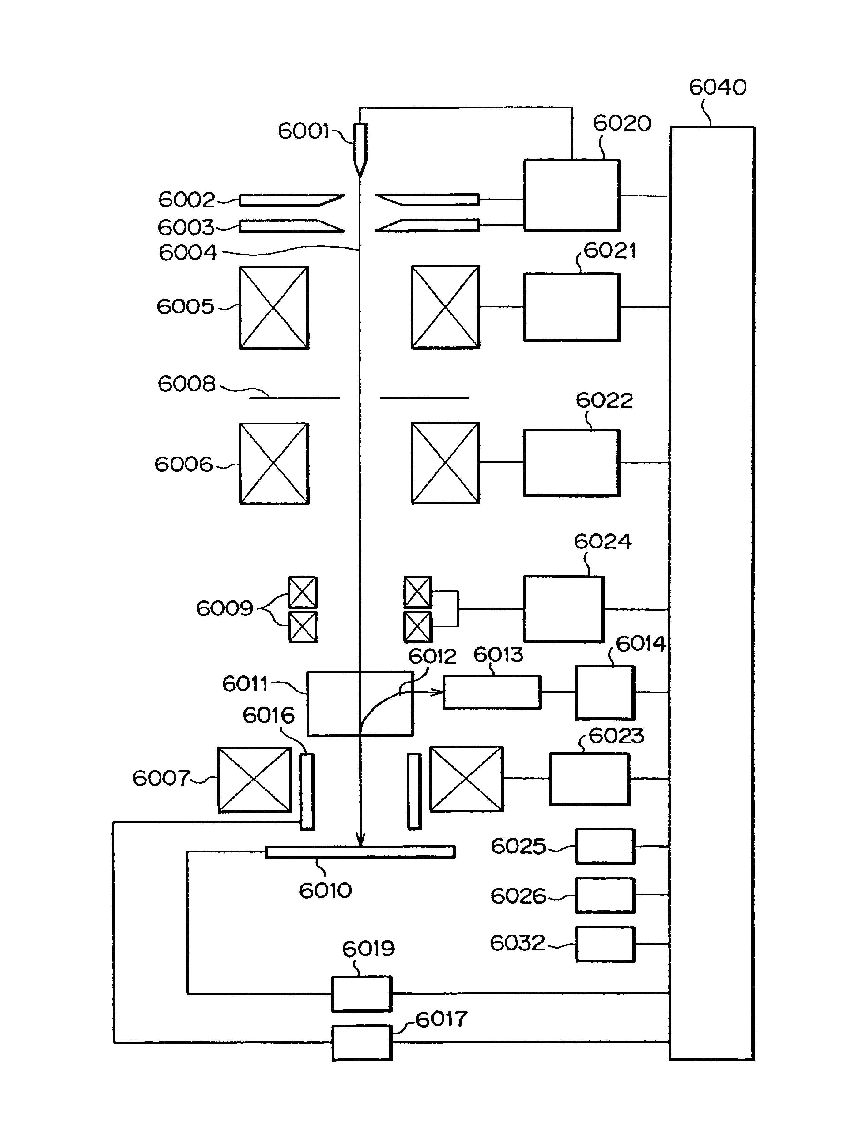
Charged particle beam apparatus
a charge-pulverized particle and beam technology, applied in the direction of beam deviation/focusing by electric/magnetic means, instruments, image enhancement, etc., can solve the problems of not being able to observe the details of the sample surface, the surface of the sample and the bottom surface of the contact hole have different focal distances
- Summary
- Abstract
- Description
- Claims
- Application Information
AI Technical Summary
Benefits of technology
Problems solved by technology
Method used
Image

Examples
first embodiment
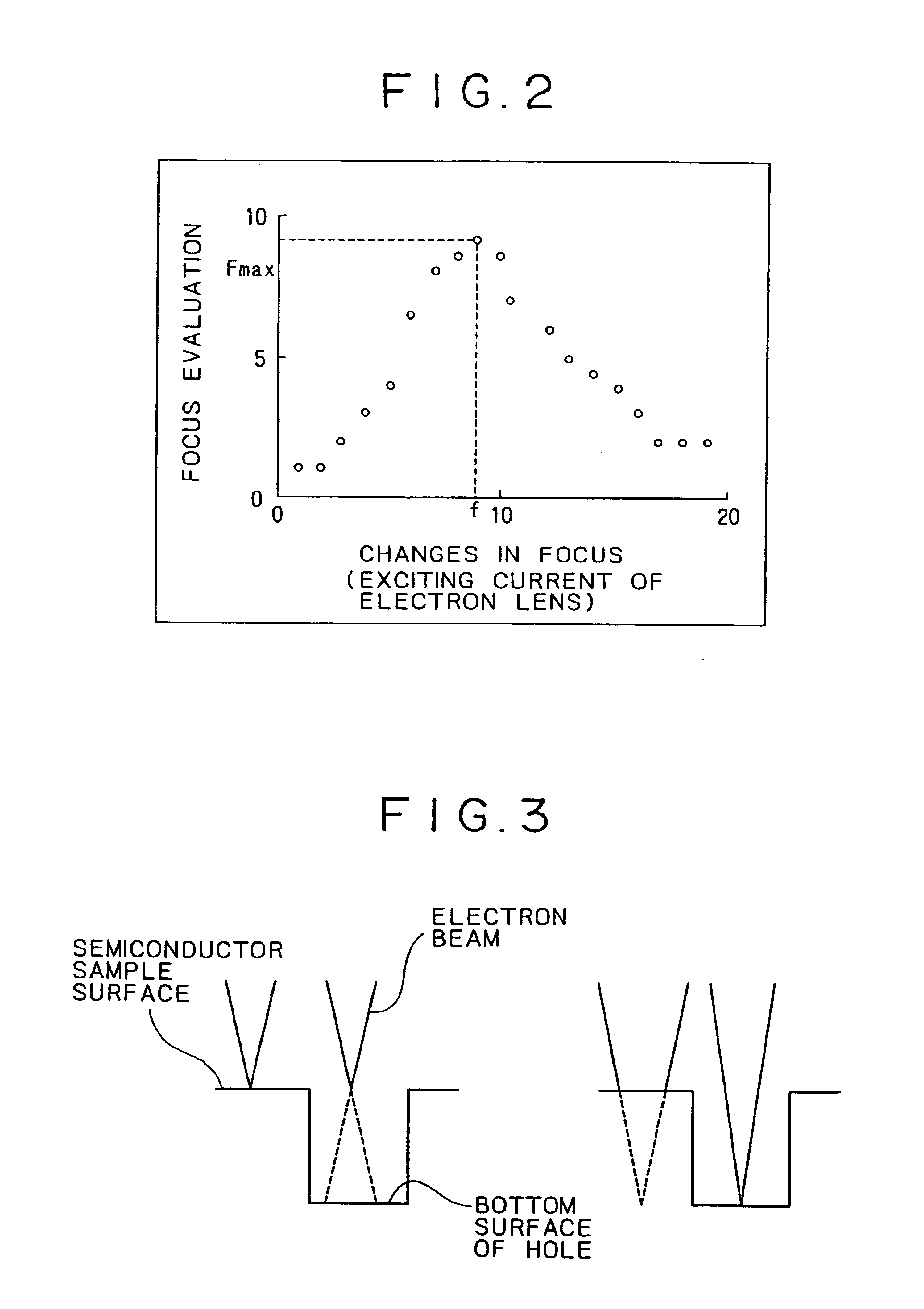
[0066]FIG. 3 is a diagram used to describe focus deviations, which are a problem to be solved by the present invention. When a semiconductor sample with a contact hole therein is scanned by a scanning electron microscope, if the electron beam is focused on the surface of the semiconductor sample, the bottom surface of a contact hole having a high aspect ratio becomes out of focus. However, if the electron beam is focused onto the bottom surface of the contact hole, on the other hand, the surface of the sample becomes out of focus. Automatic focus control functions currently incorporated in scanning electron microscopes cannot handle a local focus deviation such as this one, and can only calculate a sample surface or some average position as a focal position.
[0067]FIG. 4 is a schematic diagram for describing creation of a composite image according to the present invention. Using the semiconductor sample with contact holes therein described in FIG. 3, two images are captured: one in w...
second embodiment
[0077]FIG. 8 is a flowchart showing a flow of processes in which image acquisition, extraction of in-focus portions, and creation of a composite image are performed in parallel according to an embodiment of the present invention. Numerical 813 indicates a process in which a focal position, which can be represented by an exciting current, is varied with time.
[0078]Description will be made of processes performed as time elapses, taking processes at steps 801 through 812 as examples. An image A1 at step 801 is captured at time a1. A differential absolute value image ΔA1 of the image A1 is created at step 803 before the next image capture at time a2, and an image A2 at step 802 is captured at time a2. Before the next image capture at time a3, a differential absolute value image ΔA2 is created at step 804, and the differential absolute value imageΔA1 at step 803 is compared with the differential absolute value imageΔA2 at step 804, and at step. 805, an image ΔA1 each of whose pixels is a...
third embodiment
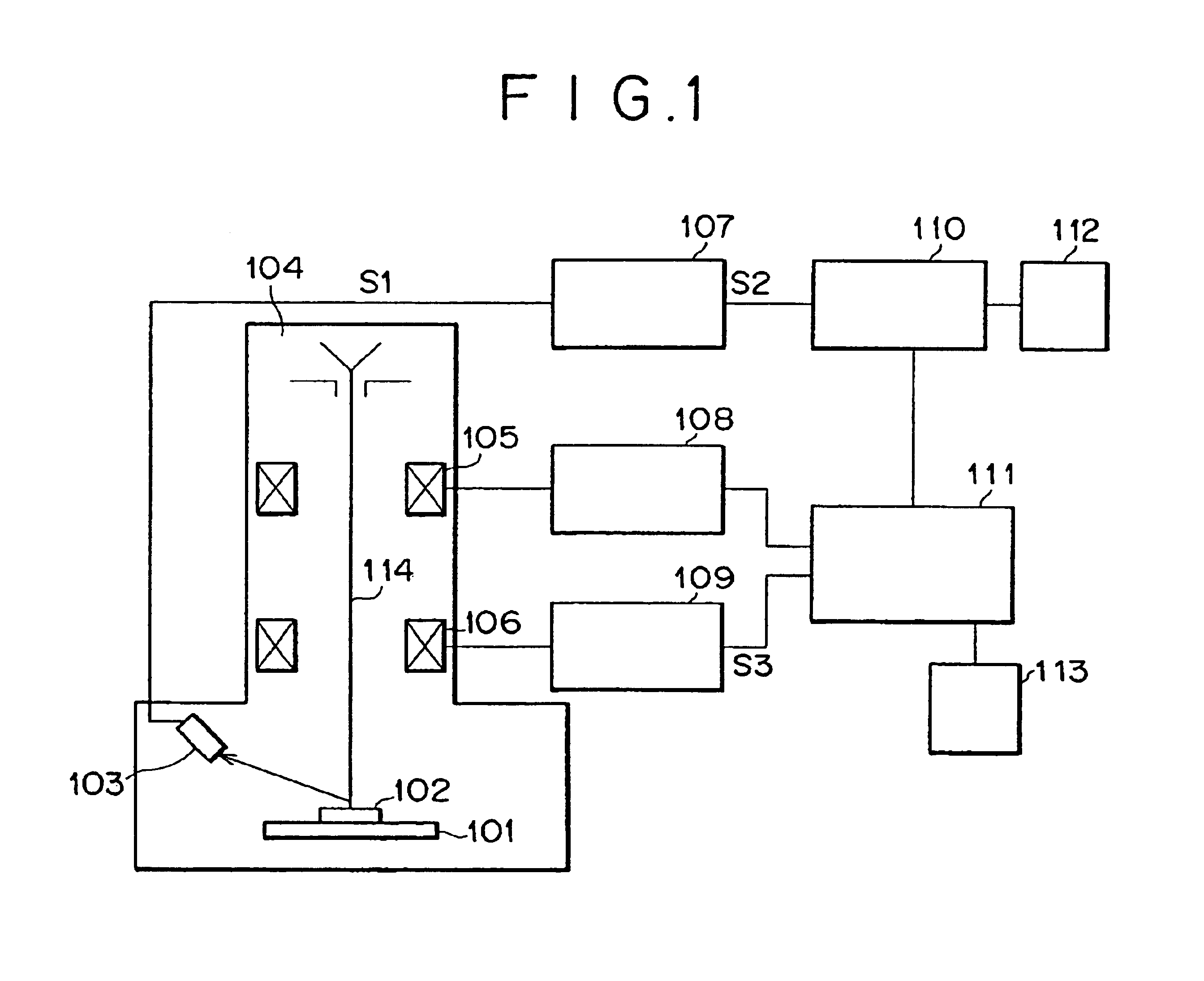
[0080]FIG. 14 is a diagram showing an indication example for a display device 112 for an apparatus according to an embodiment of the present invention. This indication example shows a composite image of a contact hole formed in a semiconductor wafer. An apparatus according to this embodiment has almost the same configuration as that described by use of FIG. 1, and, therefore, the description provided earlier will not be repeated.
[0081]Incidentally, this apparatus embodiment is provided with a pointing device (now shown) for moving a cursor 1401 on the display screen of the display device 112. This pointing device is used to select a specific area on the display screen. This apparatus embodiment has the function of replacing an area selected by this pointing device with another image. This function will be described by way of example.
[0082]The display device 112 shown in FIG. 14 is displaying an image of a contact hole formed in a semiconductor wafer. The above composition processes ...
PUM
 Abstract
Description
Claims
Application Information