Method of making an electronic contact

a technology of electronic contact and contact plate, which is applied in the field of contact, can solve the problems of thermal cycling strain on the connection, varying degrees of misalignment, and interference with the connection, and achieve the effects of reliable contact, reliable bonding, and effective scraping action

Inactive Publication Date: 2005-09-06
TESSERA INC
View PDF108 Cites 6 Cited by
  • Summary
  • Abstract
  • Description
  • Claims
  • Application Information

AI Technical Summary

Benefits of technology

[0018]In connectors according to this aspect of the invention, the regular distribution of asperities on the contact portions assures that the asperities are present on most or all of the contact portions even where the spacings between adjacent asperities are large relative to the size of the contact portions themselves. Stated another way, there is no need to pack the surface with closely spaced asperities in order to assure that each contact portion is provided with an asperity. Accordingly, each asperity may stand out from the base surface unencumbered by surrounding asperities This promotes effective scraping action, particularly in the case of very small contacts and asperities.
[0019]A further aspect of the present invention, provides methods of engaging a microelectronic element with a connector. Such methods include the step of moving the microelectronic element relative to the body of the connector so that asperities carried on contacts included in the connector scrape electrical elements, such as leads or contact pads, on the sharp edges on the tips of the asperities engage and scrape the conduct element of the microelectronic device. Preferably, the contact portions include flexible tabs and the asperities are disposed on the flexible tabs. During the engagement step, the tabs are distorted by engagement with the mating electrical mating elements of the microelectronic device, so that the projections urge the asperities into engagement with the contact elements. The method according to this aspect of the present invention may further include the step of forming a permanent metallurgical bond between the contacts and the terminals of the microelectronic element. The bonding step can be performed by activating an electrically conductive material carried by the contacts or by the engaged elements of the microelectronic device. Alternatively or additionally, the method may include the step of actuating the microelectronic element by applying signals through the contacts and the engaged elements of the microelectronic device without formation of a metallurgical bond or before such a bond is formed. Thus, the microelectronic element and its engagement with the contacts can be tested before permanent bonding. Here again, the scraping action provided by the sharp fractures on the asperities promotes reliable contact before bonding, as well as reliable bonding.
[0023]The step of depositing the etch-resistant tip material desirably is performed by applying a resist to the top surface of the sheet and then exposing the resist either to radiant energy in a pattern constituting the positive or negative image of the spots or else exposing the resist to energetic, charged particles, such as alpha particles, also in a pattern corresponding to a positive or negative image of the spots. The exposed resist is then developed and treated to remove either the exposed or unexposed regions leaving either a positive or negative image of the spots. The resist itself may serve as the etch-resistant material, in which case the resist is later removed after formation of the asperities. Alternatively, the resist may be used to control deposition of an etch-resistant metal in an electroplating step. Use of energetic charged particles such as alpha particles to expose the resist is particularly advantageous where the sheet is embossed or otherwise non-planar at the time of the exposing step.

Problems solved by technology

Further, such connections often are subject to thermal cycling strains as temperatures within the assembly change.
Such tolerances may cause varying degrees of misalignment.
Additionally, contamination on the surfaces of the mating contact parts can interfere with the connection.
All of these requirements, taken together, present a formidable engineering challenge.

Method used


Image

  • Method of making an electronic contact
  • Method of making an electronic contact
  • Method of making an electronic contact

Examples


Embodiment Construction

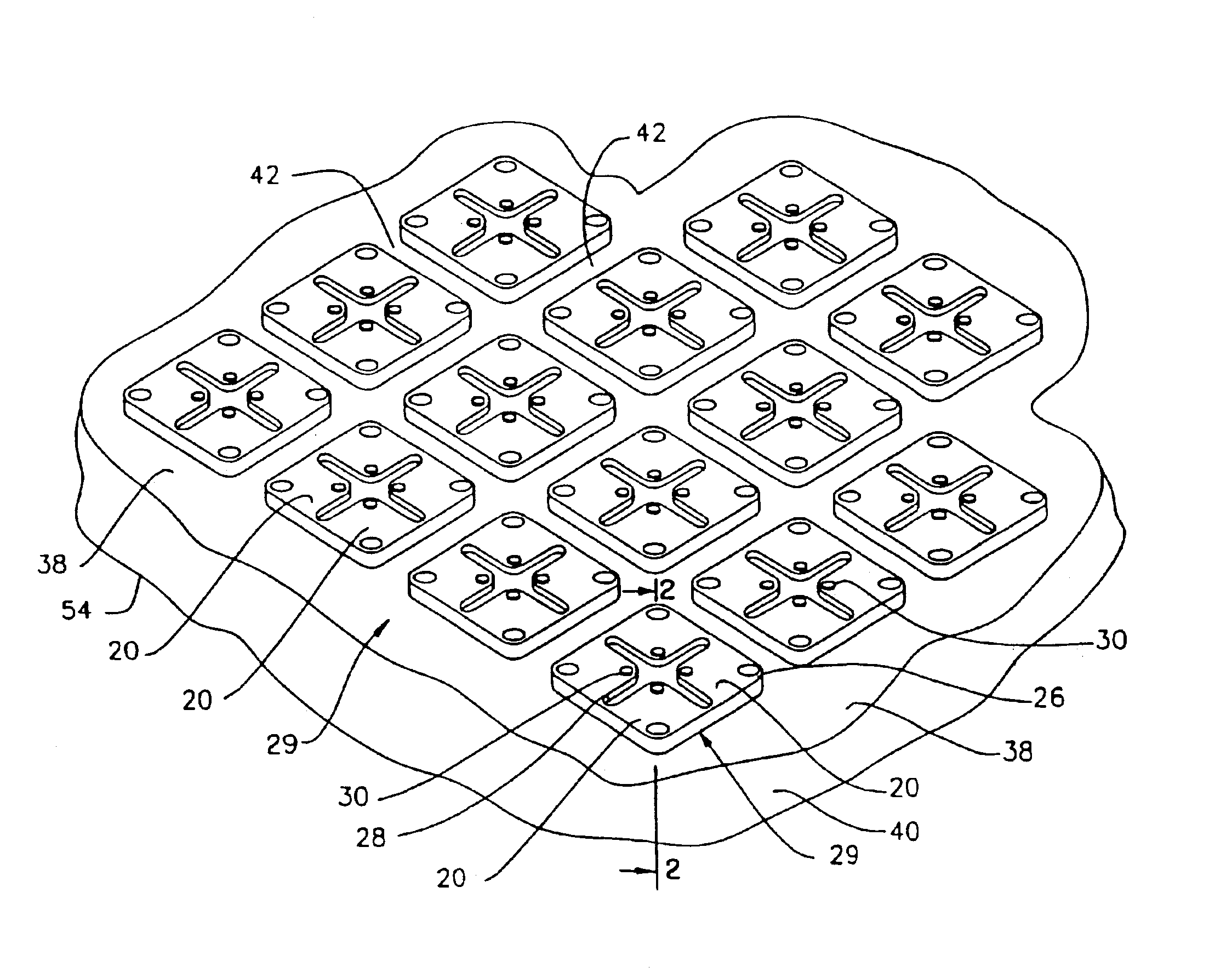
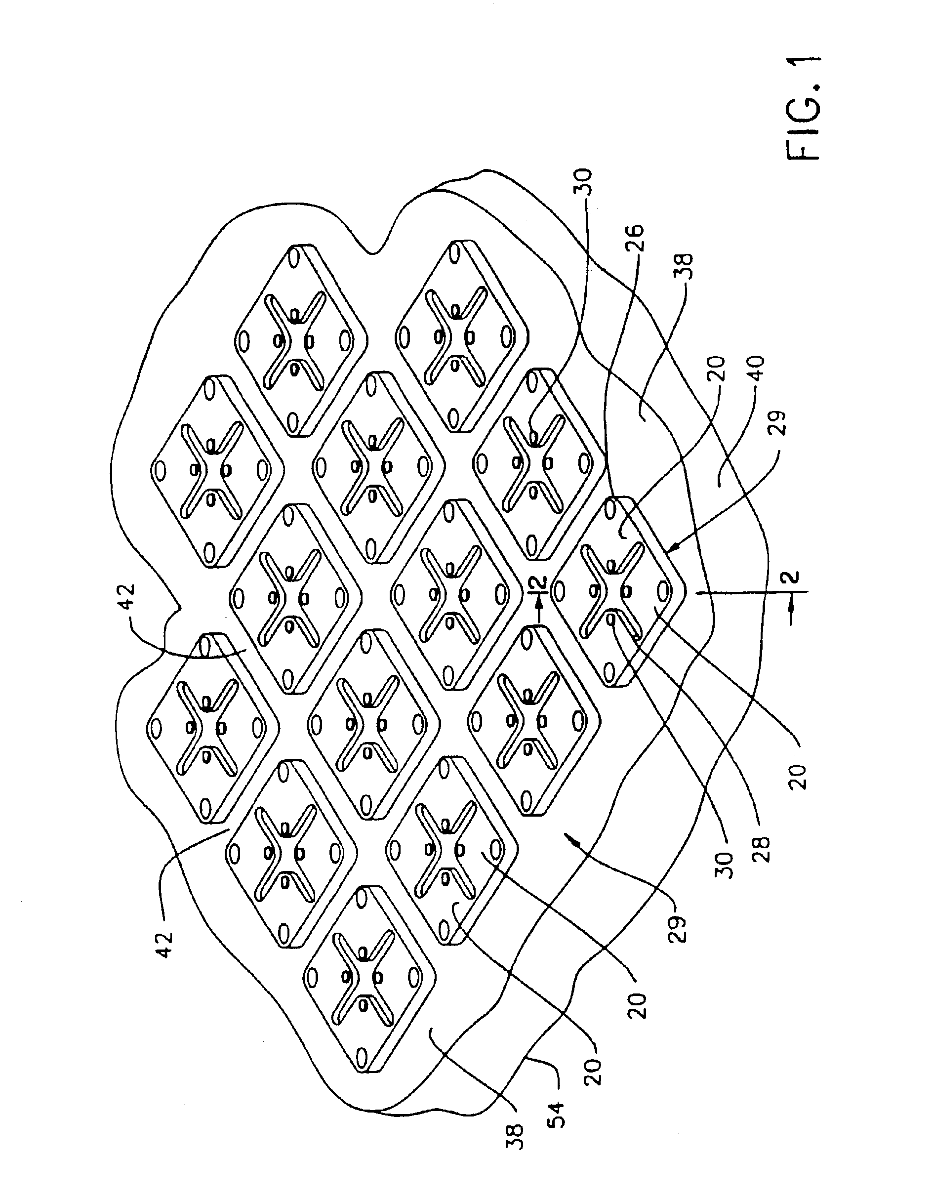
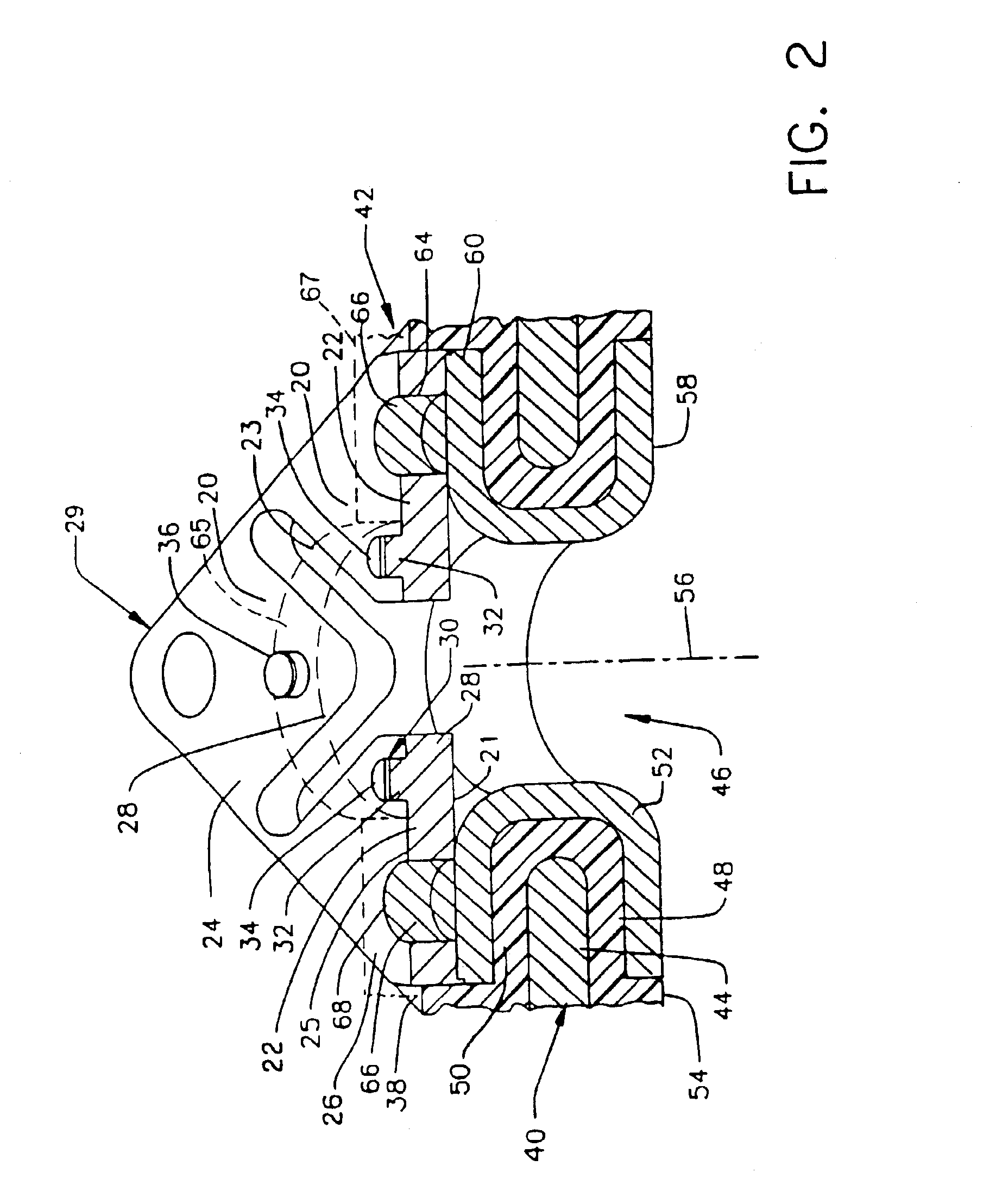
[0038]A connector according to one embodiment of the invention includes a plurality of independent, electrical contact ends 29. Each contact unit includes four contacts 20. Each contact 20 includes a small metallic tab incorporating a base layer 22 (FIG. 2) defining an upwardly facing base surface 24. The base portion of each contact desirably is formed from a resilient metal selected from the group consisting of copper, copper-bearing alloys, stainless steel and nickel. Beryllium copper is particularly preferred. The base portion desirably may be between about 10 and about 25 microns thick. A layer 25 of an etch metal such as nickel used in the contact formation process as further described below may be disposed on base surface 24. Layer 25 desirably is between about 0.5 and 2.0 microns thick. Each such tab is joined to a generally square, ring-like anchor portion 26 integral with the tab. Each tab has a tip 28 at the end of the tab remote from the anchor portion.

[0039]Four tabs ex...


PUM

PropertyMeasurementUnit
center-to-center distanceaaaaaaaaaa
peak-to-peak distanceaaaaaaaaaa

Abstract

Microelectronic contacts, such as flexible, tab-like, cantilever contacts, are provided with asperities disposed in a regular pattern. Each asperity has a sharp feature at its tip remote from the surface of the contact. As mating microelectronic elements are engaged with the contacts, a wiping action causes the sharp features of the asperities to scrape the mating element, so as to provide effective electrical interconnection and, optionally, effective metallurgical bonding between the contact and the mating element upon activation of a bonding material.

Description

[0001]This application is a divisional application of application Ser. No. 09 / 752,992 filed Jan. 2, 2001, now abandoned, which is a divisional of application Ser. No. 08 / 845,014 filed on Apr. 22, 1997, now U.S. Pat. No. 6,205,660, which claims the benefit of application Ser. No. 08 / 306,205 filed on Sep. 14, 1994, now U.S. Pat. No. 5,632,631 which is a continuation-in-part of application Ser. No. 08 / 254,991, filed on Jun. 7, 1994, now U.S. Pat. No. 5,802,699.BACKGROUND OF THE INVENTION[0002]The present invention relates to contacts for microelectronic devices such as semiconductor chips and the associated circuit panels, connectors and related devices to methods of making and using such contacts, and to components such as sockets and other connectors including such contacts.[0003]Microelectronic circuits require numerous connections between elements. For example, a semiconductor chip may be connected to a small circuit panel or substrate, whereas the substrate may in turn be connecte...

Claims


Application Information

Patent Timeline
Patent Type & Authority Patents(United States)
IPC IPC(8): G01R1/04G01R1/067G01R1/02G01R1/073H01L21/48H01L21/02H01L23/48H01L23/498H01R12/00H01R13/24H01R12/16H01R13/22H05K7/10H05K3/32H05K3/34H01R4/02H05K3/40H05K1/11B23K1/19G01R3/00G01R31/28H01R12/52H01R12/57H01R12/70H01R12/71H01R43/16H05K7/08
CPCG01R1/0466G01R1/06744G01R1/07357H01L21/4853H01L23/49816H01L23/49827H01L24/72H01R9/091H01R12/57H01R13/2407H01R13/2464H01R13/2485H05K3/326H05K3/3436H05K7/1069H05K7/1084H01R12/52H01R12/714H01R12/7076Y10T29/49126G01R1/06733G01R3/00H01L2224/16H01L2924/01004H01L2924/01013H01L2924/01015H01L2924/01027H01L2924/01029H01L2924/01032H01L2924/01039H01L2924/01046H01L2924/01049H01L2924/01074H01L2924/01075H01L2924/01078H01L2924/01079H01L2924/01082H01L2924/01322H01L2924/14H01L2924/30107H01R4/028H05K1/118H05K3/3431H05K3/4092H05K2201/0382H05K2201/0397H05K2201/1059H05K2201/10734H01L2924/01005H01L2924/01006H01L2924/01033H01L2924/01047H01L2924/01076H01L2224/16237H01L2224/8114G01R1/06727Y10T29/4921Y10T29/49224Y10T29/49155Y10T29/49222Y10T29/49156Y10T29/49117Y10T29/49204G01R1/06711H01L24/81H01L2224/45144H01L2224/81385H01L2224/81899H01L2924/12042Y02P70/50H01L2924/00
Inventor FJELSTAD, JOSEPHSMITH, JOHN W.DISTEFANO, THOMAS H.ZACCARDI, JAMESWALTON, A. CHRISTIAN
Owner TESSERA INC
Why Eureka
Try Eureka