
IC package, optical transmitter, and optical receiver

a technology of optical transmitter and optical receiver, applied in the field of ic packages, can solve the problems of increasing transmission loss, difficult to transmit a wide-band signal including high-frequency components such as microwaves or miliwaves over a wide frequency band, and slight so as to improve the manufacturability of ic packages and reduce the deterioration of the transmission characteristics of high-frequency signals

Inactive Publication Date: 2005-09-06
MITSUBISHI ELECTRIC CORP
View PDF16 Cites 0 Cited by
  • Summary
  • Abstract
  • Description
  • Claims
  • Application Information

AI Technical Summary

Benefits of technology

[0017]The present invention is proposed to solve the above-mentioned problems, and it is therefore an object of the present invention to provide an IC package which provides slight deterioration of the transmission characteristics of high-frequency signals, and which offers good manufacturability while permitting downsizing of the IC package, and an optical transmitter and an optical receiver which employ the IC package.
[0035]Accordingly, in accordance with the present invention, the deterioration of the transmission characteristics of high-frequency signals can be reduced, and the IC package can be downsized. Furthermore, the manufacturability of the IC package can be improved by enabling the mounting of the IC package on the circuit board by reflow soldering.

Problems solved by technology

However, when such an IC package structure is adopted, it is difficult to transmit a wide-band signal including high-frequency components such as microwaves or miliwaves over a wide frequency band from DC level to several tens of GHz with slight deterioration of the transmission characteristics of high-frequency signals.
Furthermore, since the transmission path for high frequencies becomes long by the connection length L1 of the leads 45 and the line length L2 from the junction to the BGA and the transmission loss increases with the increase in the length of the transmission path, the transmission characteristics of high-frequency signals is further deteriorated.
Therefore, the IC package 20 increases in size and wire bonding or ribbon bonding is needed for the connection between the plurality of leads and an external circuit, thereby deteriorating the manufacturability.
Furthermore, the second problem with the prior art IC package 20 is that when all input / output terminals of the IC package 20 with a lot of pins, such as MUX and DEMUX, are constructed of feedthroughs which provide slight deterioration of the transmission characteristics of high-frequency signals, the IC package 20 increases in size and a plurality of leads or the like are needed for the connection with an external circuit, thereby deteriorating the manufacturability.

Method used


Image

  • IC package, optical transmitter, and optical receiver
  • IC package, optical transmitter, and optical receiver
  • IC package, optical transmitter, and optical receiver

Examples


embodiment 1

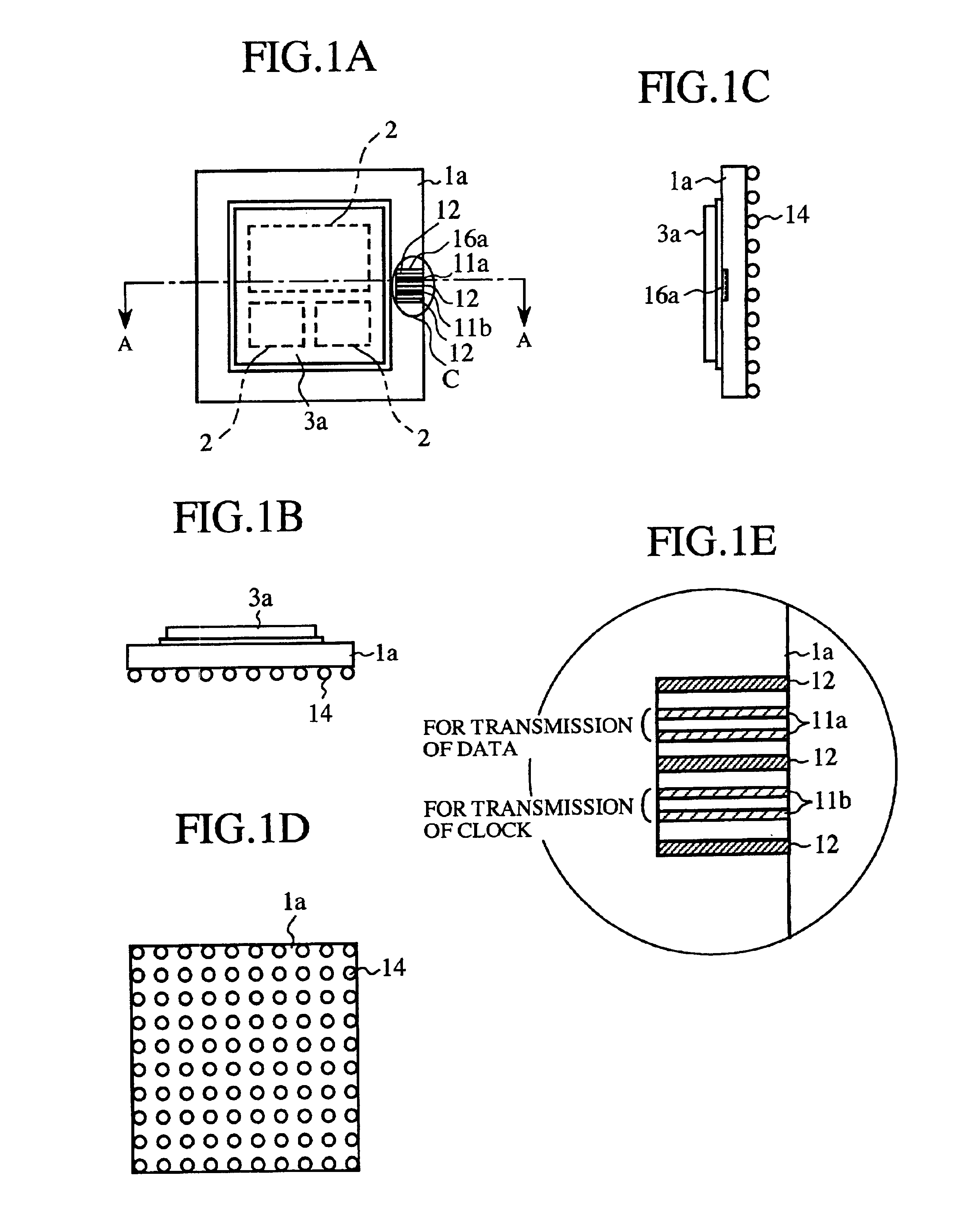
[0053]Referring now to FIGS. 1A to 1E, there is illustrated an IC package according to a first embodiment of the present invention. FIG. 1A is a top plan view of the IC package, FIGS. 1B and 1C are side views of the IC package, FIG. 1D is a bottom plan view of the IC package, and FIG. 1E is a partially enlarged detail view of a circle C of FIG. 1A including an exposed portion of two differential pairs of lines of the IC package. In FIGS. 1A to 1E, a group-of one or more bare chips and a plurality of bumps are the same as those shown in FIG. 13 of the prior art IC package, and these components are designated by the same reference numerals and therefore the explanation of the components will be omitted hereafter.

[0054]Furthermore, in FIGS. 1A to 1E, reference numeral 1a denotes a chip carrier, reference numeral 3a denotes a metallic lid, reference numerals 11a and 11b denote the two differential pairs of lines (conductive lines) each of which is disposed on an upper surface (first sur...

embodiment 2

[0091]FIGS. 11A to 11D are views showing the structure of an IC package according to a second embodiment of the present invention. FIG. 11A is a top plan view of the IC package, FIGS. 11B and 11C are side views of the IC package, and FIG. 11D is a bottom plan view of the IC package. In FIGS. 11A to 11D, a plurality of bare chips 2 and a plurality of bumps 14 are the same as those of the first embodiment shown in FIGS. 1A to 1E, and therefore the explanation of those components will be omitted hereafter. Reference character 1b denotes a chip carrier which is similar to the chip carrier 1a of the first embodiment shown in FIGS. 1A to 1E, and reference character 3c denotes a metallic lid which is similar to the metallic lid 3a of the first embodiment shown in FIGS. 1A to 1E.

[0092]In this embodiment, two differential pair of lines 11a and 11b through which high-frequency signals are transmitted are exposed on a surface of a groove 16b formed in a lower surface (second surface) of the ch...


PUM


Abstract

There is provided an IC package provided with one or more bare chips mounted on a chip carrier, a plurality of first bumps each for connecting a chip electrode to a conductive pad disposed on an upper surface of the chip carrier, a plurality of second bumps each connected to a conductive pad disposed on a bottom surface of the chip carrier, and a plurality of vias for connecting between conductive pads disposed on the upper and bottom surfaces of the chip carrier. A differential pair of lines are exposed on the upper surface of the chip carrier. High-frequency signals to be processed by the one or more bare chips are transmitted by way of the differential pair of lines, and other signals are transmitted by way of the plurality of second bumps.

Description

BACKGROUND OF THE INVENTION[0001]1. Field of the Invention[0002]The present invention relates to an IC package having a lot of pins, and an optical receiver and an optical transmitter each of which employs the IC package.[0003]2. Description of the Prior Art[0004]Referring now to FIGS. 13A to 13C, there is illustrated a prior art IC package having a lot of pins and including such a circuit as a multiplexer (MUX) for use in an optical transmitter or a demultiplexer (DEMUX) for use in an optical receiver. FIG. 13A is a top plan view of the IC package, FIG. 13B is a side view of the IC package, and FIG. 13C is a bottom plan view of the IC package.[0005]In FIGS. 13A to 13C, reference numeral 1 denotes a chip carrier constructed of low temperature cofired ceramic in which a plurality of dielectric substances each of which includes conductive pads, vias (or connection holes), conductive lines, and grounded conductors are laminated. For example, the chip carrier 1 has a 10 mm to 20 mm squa...

Claims


Application Information

Patent Timeline
Patent Type & Authority Patents(United States)
IPC IPC(8): H01L23/58H01L23/66H01S5/022H01L31/02
CPCH01L23/66H04B10/69H01L2224/16235H01L2224/16225H01L2224/48091H01L2224/49175H01L2224/73204H01L2224/73253H01L2924/01046H01L2924/01079H01L2924/09701H01L2924/14H01L2924/1423H01L2924/15311H01L2924/16152H01L2924/1903H01L2924/19107H01L2924/30107H01L2924/3011H01L2924/3025H01L2223/6627H01L2224/32225H01L2224/45144H01L24/49H01L24/48H01L2924/00014H01L2924/00H01L2924/12042H01L24/45H01L2224/05554H01L2924/00012H01L2224/05599
Inventor NAGASE, TORUTAJIMA, MINORUTOKUMORI, NOBUHIRO
Owner MITSUBISHI ELECTRIC CORP
Learn More