Electroluminescence display device

a display device and electroluminescent technology, applied in the direction of luminescent screens, discharge tubes, instruments, etc., can solve the problems of current leakage in both tfts and increase in power consumption

Inactive Publication Date: 2005-09-06
SANYO ELECTRIC CO LTD
View PDF13 Cites 254 Cited by
  • Summary
  • Abstract
  • Description
  • Claims
  • Application Information

AI Technical Summary

Benefits of technology

[0040]Forming the emissive layer using an organic compound can be extremely advantageous in a color display device because organic compounds can provide many variations in emitted colors and can be formed from a wide selection of possible materials.

Problems solved by technology

As a result, current leaks in both TFTs when Vg=0 V.
Generation of penetration current due to such changes disadvantageously causes an increase in power consumption.

Method used


Image

  • Electroluminescence display device
  • Electroluminescence display device
  • Electroluminescence display device

Examples


Embodiment Construction

[0052]An EL display device of the present invention will now be described.

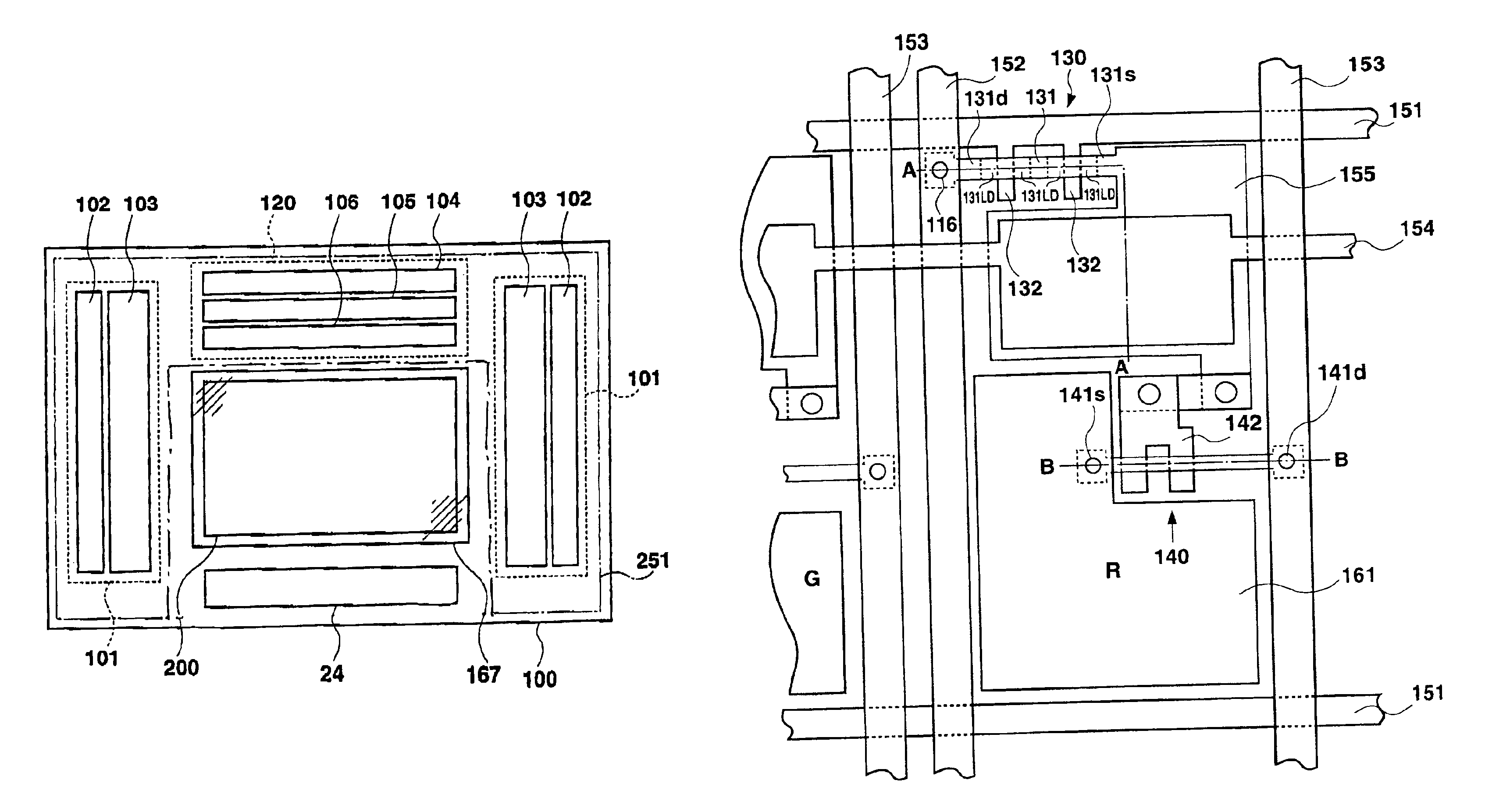
[0053]FIG. 7 shows a plan view of an organic EL display device. An example in which the EL display device of the present invention is implemented in an organic EL display device is explained referring to this figure.

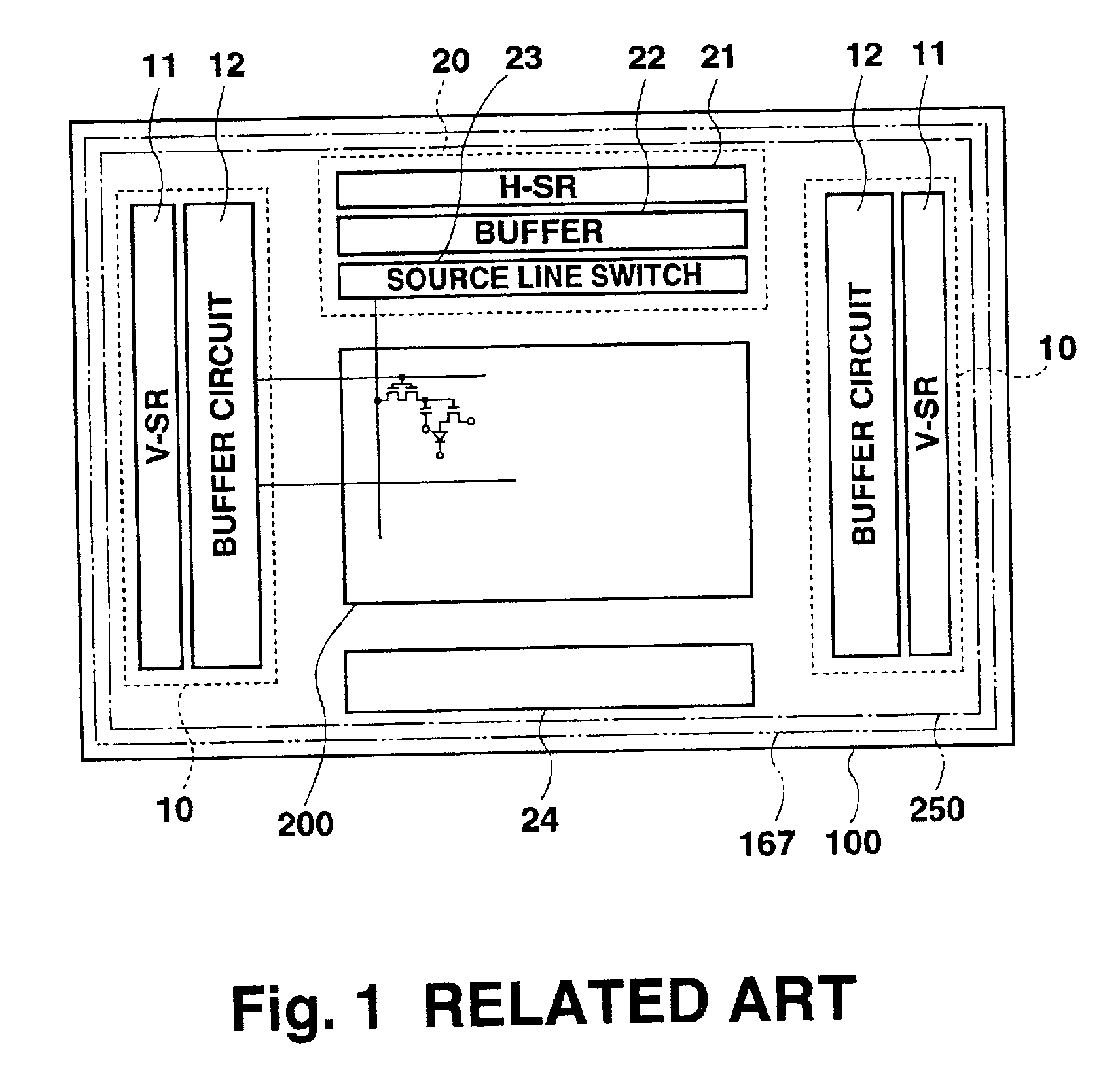
[0054]In the organic EL display device, as shown in FIG. 7, an insulator substrate 100 is provided with a peripheral drive circuit 251 including horizontal drive circuit 120 and vertical drive circuits 101 configured using third TFTs. Also formed on the insulator substrate 100 is a display pixel region 200 including display pixels of the organic EL display. The third TFTs are formed within the peripheral drive circuit region. Each vertical drive circuit 101 includes a vertical shift register (V-SR) 102 and a buffer circuit 103. A horizontal drive circuit 120 includes a horizontal shift register (H-SR) 104, a buffer 105, and a source line switch 106.

[0055]A pixel in the display pixel region 200 has ...


PUM


Abstract

An insulator substrate (110) is provided with a display pixel region (200) comprising an electroluminescence element (160) having a cathode (167), emissive layer (166), and anode (161), and with first and second TFTs for driving the element. Surrounding the display pixel region (200), a peripheral drive circuit region (251) having a third TFT for driving each pixel is further provided on the insulator substrate (110). The cathode (167) is disposed in a region other than the peripheral drive circuit region (251). With this arrangement, generation of a back channel by applying the EL element potential to the cathode is prevented in a complementary TFT employed in the peripheral drive circuit region for controlling the display region, thereby suppressing changes in threshold values due to such back channel generation. As a result, an EL display device with reduced generation of penetration current and minimized increased current consumption is achieved.

Description

BACKGROUND OF THE INVENTION[0001]1. Field of the Invention[0002]The present invention relates to an electroluminescence display device employing an electroluminescence element and a thin film transistor.[0003]2. Description of the Related Art[0004]In recent years, electroluminescence (EL) display devices comprising EL elements have gained attention as potential replacement for CRT and LCD devices. Some research has been directed to the development of EL display devices using, for example, thin film transistors (referred to hereinafter as “TFT”) as switching elements to drive the EL elements.[0005]FIG. 1 shows a plan view of a related organic EL display device.[0006]As shown in the Figure, the organic EL display device comprises a display pixel region 200 having first and second TFTs for driving an organic EL element of the display pixel. The organic EL display device further comprises a peripheral drive circuit region 250 indicated by a single-dot broken line. The peripheral drive c...

Claims


Application Information

Patent Timeline
Patent Type & Authority Patents(United States)
IPC IPC(8): H01L27/32H01L27/28G09F9/30H01L51/50H05B33/00H05B33/12H05B33/14H05B33/26
CPCH01L27/3244H01L51/5221H10K59/12H10K50/828H05B33/00
Inventor KOMIYA, NAOAKIOKUYAMA, MASAHIRO
Owner SANYO ELECTRIC CO LTD
Why Eureka
Try Eureka