Optically pumped semiconductor ring laser

a semiconductor ring laser and optical pump technology, applied in the direction of lasers, semiconductor lasers, optical resonator shape and construction, etc., can solve the problem of limit the amount of power that can be generated

Inactive Publication Date: 2005-09-06
COHERENT INC
View PDF10 Cites 46 Cited by
  • Summary
  • Abstract
  • Description
  • Claims
  • Application Information

AI Technical Summary

Benefits of technology

[0011]In one aspect, the present invention is directed to a laser, comprising at least one composite layer-structure including a multilayer semiconductor gain-structure surmounting a mirror-structure. The mirror-structure is arranged as a resonator mirror of an active unidirectional ring-resonator with the gain-structure located in the ring-resonator. The term “active” here means that the ring-resonator includes a gain-structure. The gain-st...

Problems solved by technology

At any given resonator length and mode spot size, there is a limit to the amount of power that can be generated that is imposed by a limit on the amount of pump power that can be delivered to the ...

Method used


Image

  • Optically pumped semiconductor ring laser
  • Optically pumped semiconductor ring laser
  • Optically pumped semiconductor ring laser

Examples


Embodiment Construction

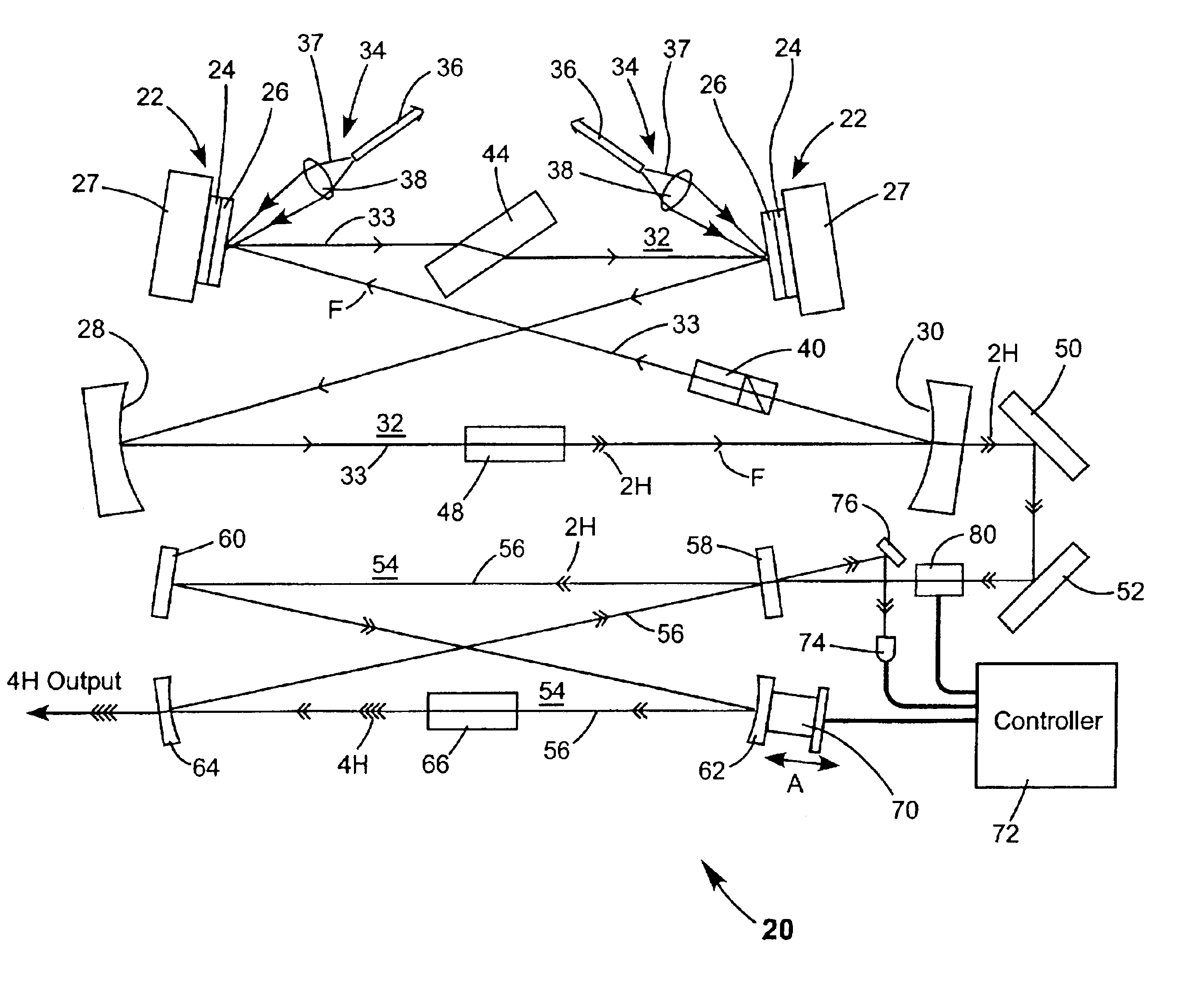
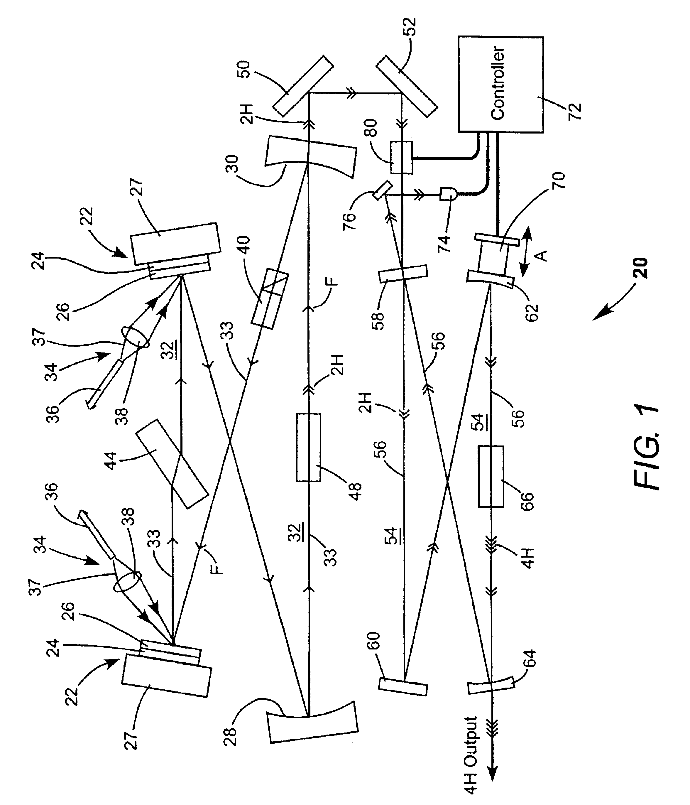
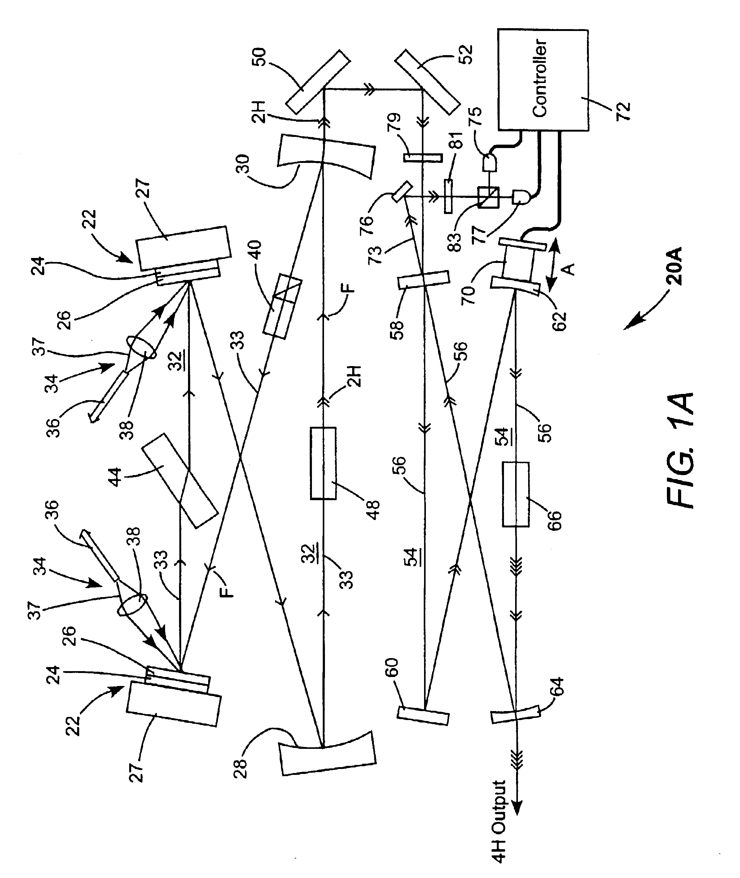
[0024]Referring now to the drawings wherein like features are designated by like reference numerals, FIG. 1 schematically illustrates a first preferred embodiment 20 of an OPS laser in accordance with the present invention. Laser 20 includes two OPS-structures 22. Each of the OPS structures is a composite layer-structure having a mirror-structure 24 surmounted by a semiconductor multilayer, surface-emitting gain-structure 26. OPS-structures 22 are each supported on a substrate or heat sink 27, with mirror-structure 24 of the OPS-structure in thermal contact with the substrate. As such OPS-structures are well known in the art, a detailed description thereof is not presented herein. A detailed description of such structures including a description of layer materials and their arrangement and heat-sink designs is provided in above-referenced U.S. Pat. No. 6,097,742, the complete disclosure of which is hereby incorporated by reference.

[0025]Mirror-structures 24 of the OPS-structures and...


PUM


Abstract

An optically pumped semiconductor laser includes an active ring-resonator having two or more optically pumped semiconductor (OPS) structures each including a mirror-structure and a multilayer gain-structure. The mirror-structures serve as fold mirrors for the resonator axis. An optically nonlinear crystal may be included in the ring-resonator for generating second-harmonic radiation from fundamental radiation generated in the resonator. Another optically nonlinear crystal may be provided for generating third-harmonic or fourth-harmonic radiation from the second-harmonic radiation. In one example, including a third-harmonic generating crystal, a passive ring-resonator partially coaxial with the active ring-resonator is provided for circulating second-harmonic radiation to provide resonant amplification of the second-harmonic radiation for enhancing third-harmonic conversion. Apparatus for automatically maintaining the passive ring-resonator in a resonant condition for the second-harmonic radiation is disclosed.

Description

TECHNICAL FIELD OF THE INVENTION[0001]The present invention relates in general to external-cavity optically-pumped semiconductor lasers (hereinafter, OPS-lasers) including a surface-emitting, semiconductor multilayer (periodic) gain-structure. The invention relates in particular to traveling-wave resonator arrangements of such lasers.DISCUSSION OF BACKGROUND ART[0002]The term OPS-lasers, as used herein, refers to a class of vertical-cavity surface-emitting semiconductor lasers wherein optical gain is provided by recombination of electrical carriers in very thin layers, for example, about 150 Ångstrom units (Å) or less, of a semiconductor material. These layers are generally termed quantum-well (QW) layers or active layers.[0003]In an OPS-laser, several QW layers, for example, about fifteen, are spaced apart by separator layers also of a semiconductor material, but having a higher conduction band energy that the QW layers. This combination of active layers and separator layers may be...

Claims


Application Information

Patent Timeline
IPC IPC(8): H01S3/10H01S3/081H01S3/082H01S3/083H01S3/0941H01S3/105H01S3/109H01S5/04H01S5/06H01S5/10H01S5/14H01S5/183H01S5/42
CPCH01S3/083H01S3/0941H01S3/109H01S5/141H01S3/07H01S3/0816H01S3/082H01S3/1003H01S3/105H01S5/041H01S5/183H01S5/423
Inventor BUTTERWORTH, STUARTCAPRARA, ANDREAAUSTIN, R. RUSSEL
Owner COHERENT INC
Why Eureka
Try Eureka