Multiplying-adding return to zero digital to analog converter circuit and method

a technology return circuit, applied in the field of digital to analog converter, can solve the problems of increasing the power consumption of the circuit, reducing the operating speed, and high power consumption of achieve the effect of reducing the switching glitches in the output of the dac and removing the digital adder circuitry

Inactive Publication Date: 2010-12-09
BAE SYST INFORMATION & ELECTRONICS SYST INTERGRATION INC
View PDF15 Cites 0 Cited by
  • Summary
  • Abstract
  • Description
  • Claims
  • Application Information

AI Technical Summary

Benefits of technology

[0016]A digital to analog converter (DAC) method and apparatus employs a multiplying-adding DAC, eliminating digital adder circuitry. Examples are given for multiplying a 3-bit binary number by a 2-bit binary number; however, there are no limitations to the bit-widths of the numbers to be multiplied. The multiplying-adding DAC method can be scaled up or down in bit-width by feeding the DAC with partial sums and adjusting the DAC weights accordingly. An analog to digital converter (ADC) can be placed after the DAC to generate a digital output. By multiplexing preset digital data into the DAC core for return to zero (RTZ), a true zero that is the midpoint of the DAC output range is achieved. It does not return to a rail for single-ended outputs. RTZ in DAC circuits doubles the null frequency of sin(x) / x roll-off inherent in DACs and also helps reduce switching glitches in the DAC output.

Problems solved by technology

Digital adder circuitry increases the power consumption of the circuit and reduces operating speed.
A large number of gates is involved in the complex logic required to compute this result.
This leads to high power consumption and large propagation delay which can decrease speed or necessitate pipelining.
The approach also lends itself to a long worst case slew rate.

Method used


Image

  • Multiplying-adding return to zero digital to analog converter circuit and method
  • Multiplying-adding return to zero digital to analog converter circuit and method
  • Multiplying-adding return to zero digital to analog converter circuit and method

Examples


Embodiment Construction

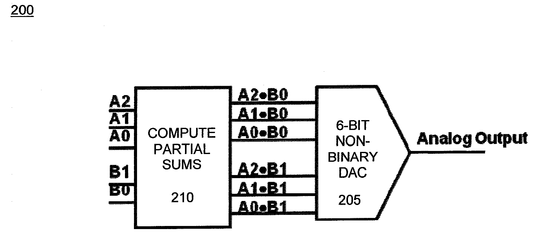
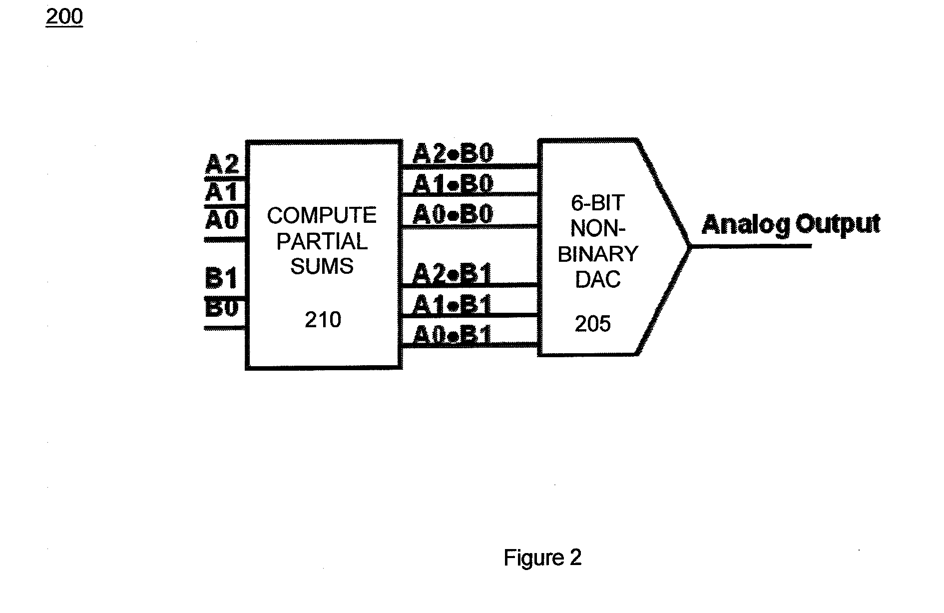
Multiplying-Adding DAC

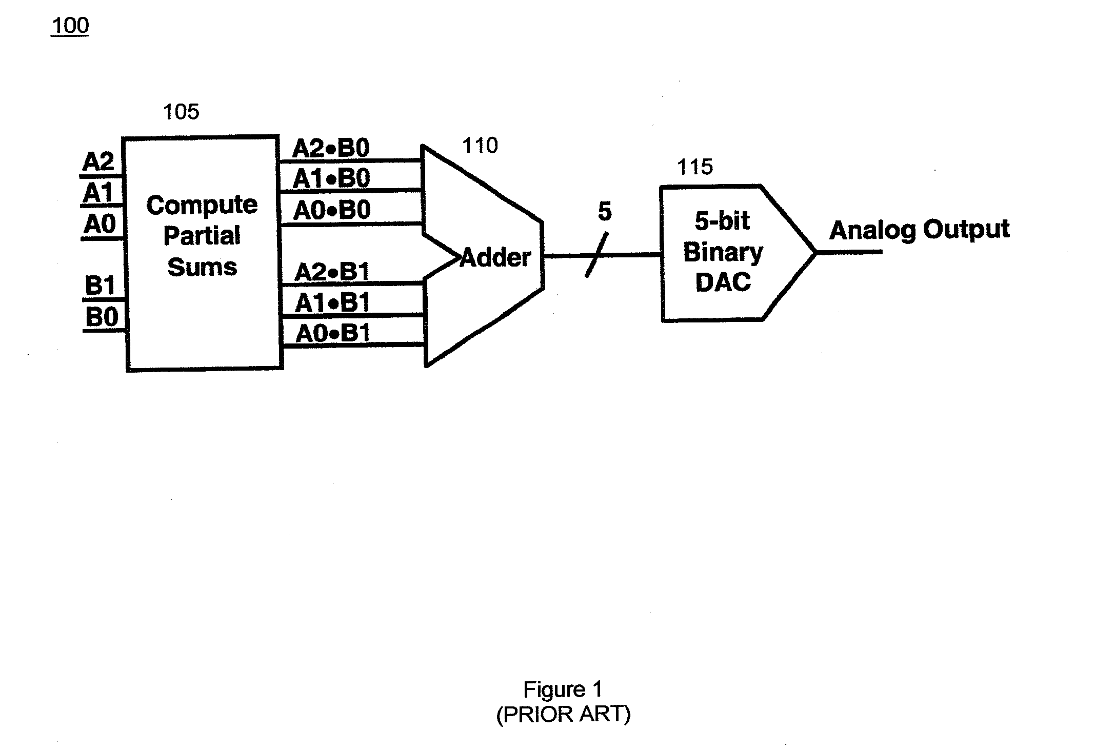
[0040]The multiplying-adding DAC eliminates digital adder circuitry. Less complex logic is used, circuitry is faster and power consumption is lower from reduced gate count. The non-binary DAC reduces skew by eliminating the weight of 16. Overall current is reduced by 10 weights, since the 16 weight is removed and extra 2 and 4 weights are added. Examples are given for multiplying a 3-bit binary number by a 2-bit binary number; however, there are no limitations to the bit-widths of the numbers to be multiplied. The multiplying-adding DAC method can be scaled up or down in bit-width by feeding the DAC with partial sums and adjusting the DAC weights accordingly. An analog to digital converter (ADC) can be placed after the DAC to generate a digital output. The approach is not limited to DDS circuits; it can be used in any circuit where a digital or analog multiplication output is desired. The following figures include embodiments demonstrating the multiplying-addin...


PUM


Abstract

A digital to analog converter (DAC) method and apparatus employs a multiplying-adding DAC, eliminating digital adder circuitry. Examples are given for multiplying a 3-bit binary number by a 2-bit binary number; however, there are no limitations to the bit-widths of the numbers to be multiplied. The multiplying-adding DAC method can be scaled up or down in bit-width by feeding the DAC with partial sums and adjusting the DAC weights accordingly. An analog to digital converter (ADC) can be placed after the DAC to generate a digital output. By multiplexing preset digital data into the DAC core for return to zero (RTZ), a true zero that is the midpoint of the DAC output range is achieved. It does not return to a rail for single-ended outputs. RTZ in DAC circuits doubles the null frequency of sin(x)/x roll-off inherent in DACs and also helps reduce switching glitches in the DAC output.

Description

STATEMENT OF GOVERNMENT INTEREST[0001]The invention was made with United States Government support under Contract No. DAAD17-02-C-0115 awarded by the US Army and under a separate, classified contract. The United States Government has certain rights in this invention.FIELD OF THE INVENTION[0002]The present invention relates to digital to analog converters (DACs), and more particularly, to a method and apparatus for enhanced performance through improved spurious free dynamic range (SFDR) and accurate return to zero (RTZ) performance.BACKGROUND OF THE INVENTION[0003]DACs are used in an increasing number of applications, many requiring lower power consumption and higher operating frequencies. Direct Digital Synthesis (DDS) is one of these applications. Basic DDS circuits include an electronic controller, random access memory, a frequency reference, a counter, and a DAC. Some versions of DDS circuits include random access memory (RAM).Multiplying-Adding [0004]Within direct digital synthe...

Claims


Application Information

Patent Timeline
Patent Type & Authority Applications(United States)
IPC IPC(8): H03M1/66
CPCH03M1/002H03M1/08H03M1/747H03M1/745H03M1/687
Inventor TURNER, STEVEN E.ELDER, JR., RICHARD B.
Owner BAE SYST INFORMATION & ELECTRONICS SYST INTERGRATION INC
Why Eureka
Try Eureka