Substrate for integrating and forming a thin film semiconductor device thereon

Inactive Publication Date: 2005-09-13
SONY CORP
View PDF22 Cites 77 Cited by
  • Summary
  • Abstract
  • Description
  • Claims
  • Application Information

AI Technical Summary

Benefits of technology

[0024]According to this invention, in the preparatory step before forming the thin film transistor, a manufacturing substrate, for example, made of glass is previously appended to a product substrate, for example, made of a plastic material for reinforcement. Subsequently, a thin film transistor is integrated and formed on a product substrate made, for example, of a plastic material. In this case, since the product substrate made, for example, of a plastic material or the like is backed by the manufacturing substra

Problems solved by technology

If the substrate is deformed, such as by warping, automatic transportation using a manipulator is not possible.
Therefore, manufacturing conditions required for the substrate and conditions for the products do not often agree with each other, and there is a market complaint against the products.
However, in view of the product conditions, the glass substrate has a drawbacks of heavy weight and easy cracking.
Actually, the glass substrate is heavy, sensitive to deformation and likely to be broken by dropping.
That is, there is a difference between restrictions due to manufacturing conditions and preferred characteristics required for the products, and it is difficult to satisfy both of the conditions or characteristics, and this is left still unresolved.
However, the plastic substrate suffers from a larger deformation compared with the glass substrate, and no satisfactory products have been obtained at present (N. D. Young, et al., Euro Display '96 Digest, 555, 1996).
However, this method is complicated in the transfer step and involves a problem in view of the productivity.
Further, since the provisional substrate used for forming the thin film transistor and a substrate for mounting the thin film transistor as a product are different, characteristic are liable to fluctuate in the thin film transistor in view of the problems, such as stresses and the like.

Method used


Image

  • Substrate for integrating and forming a thin film semiconductor device thereon
  • Substrate for integrating and forming a thin film semiconductor device thereon
  • Substrate for integrating and forming a thin film semiconductor device thereon

Examples


Embodiment Construction

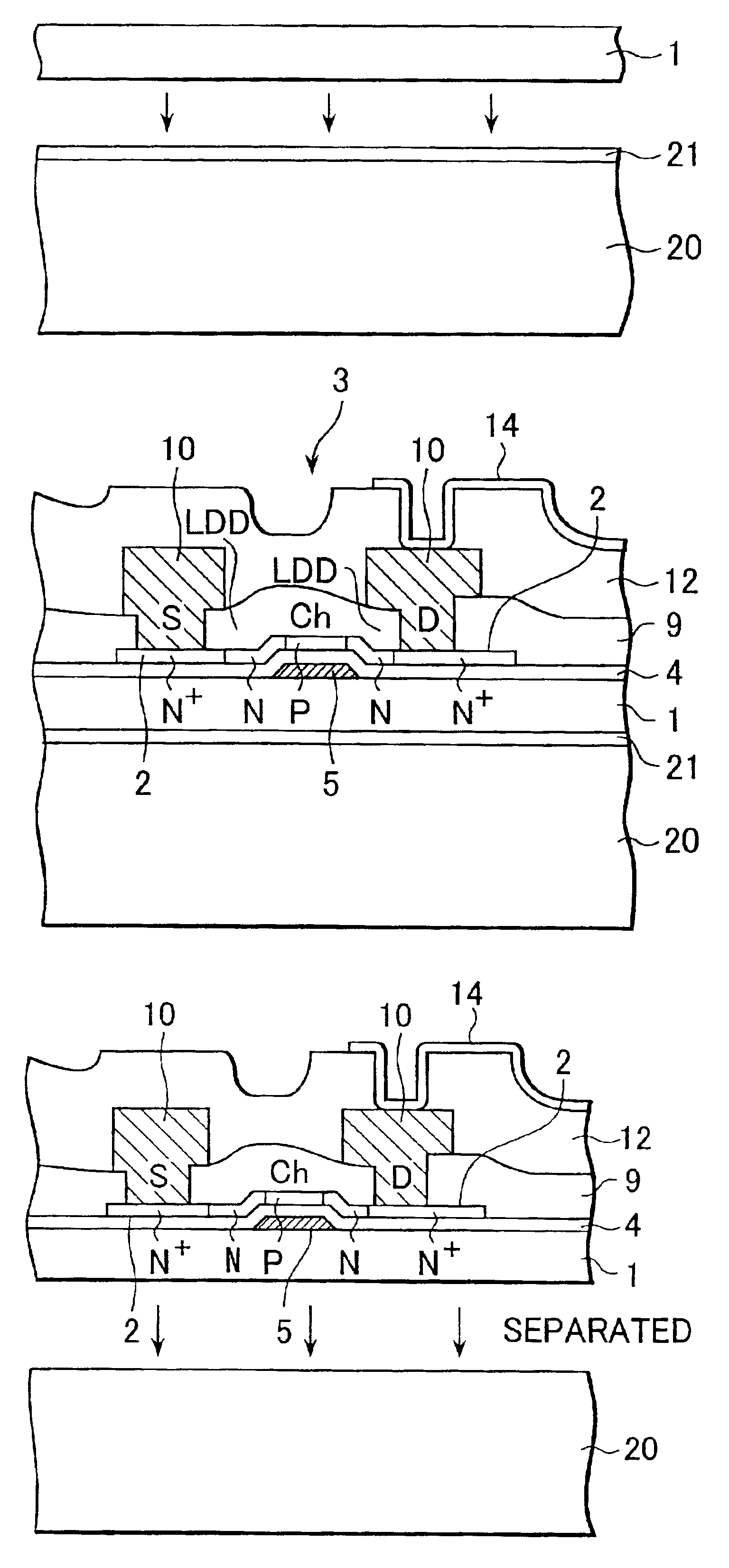
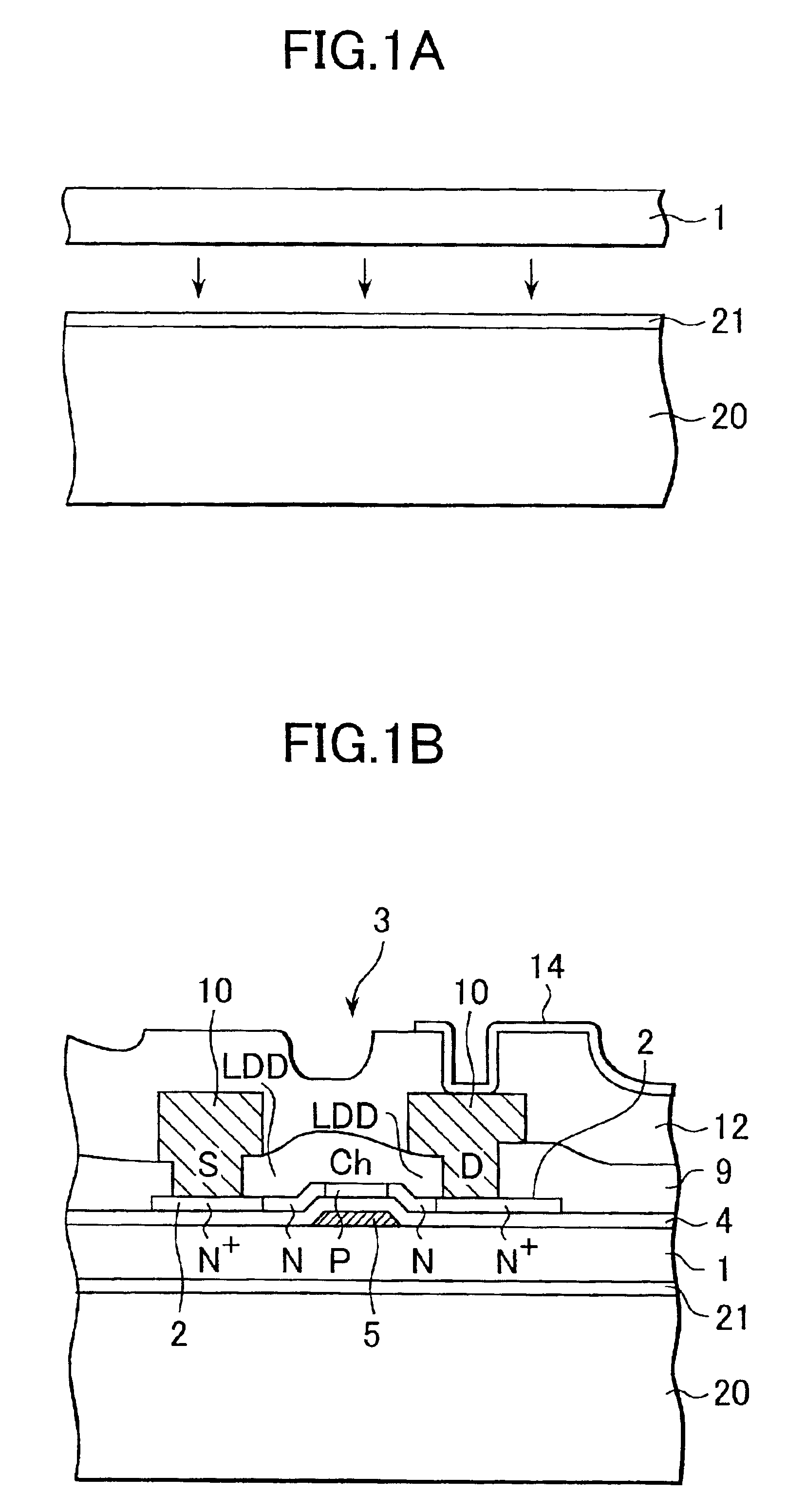
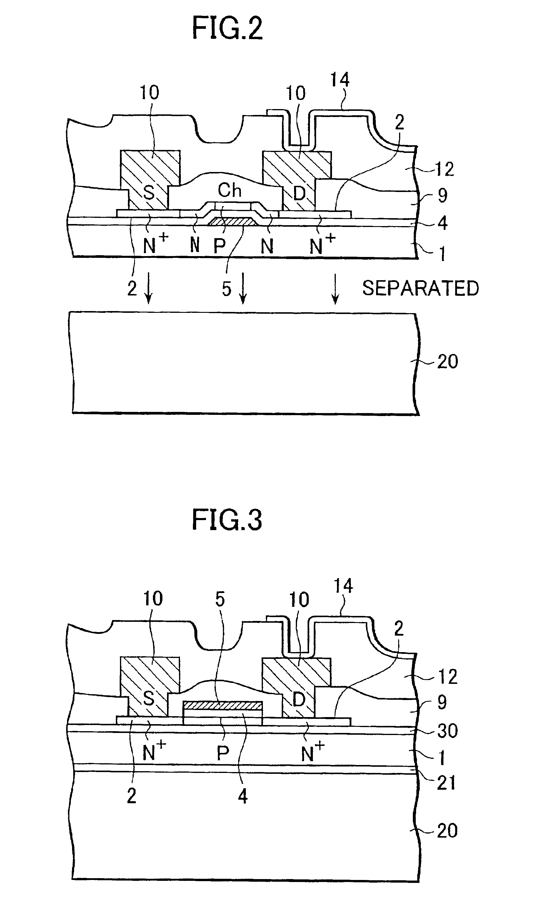
[0030]Preferred embodiments of this invention are to be described in detail with reference to the drawings. FIGS. 1A and 1B are an example of schematic step charts illustrating a method of manufacturing a thin film semiconductor device according to this invention. At first, as shown in FIG. 1A, a manufacturing substrate 20 having characteristics durable to the process for forming a thin film transistor and a product substrate 1 having characteristics suitable to direct mounting of a thin film transistor are prepared. In the preparatory step, a manufacturing substrate 20, for example, made of an inorganic material, such as glass, and a product substrate 1 made of an organic material, such as plastic, are prepared. In this embodiment, non-alkali glass is used as the manufacturing substrate 20. The heat resistance of the non-alkali glass is about 500° C. The standard thickness for the manufacturing substrate 20 is, for example, 0.7 mm. If it is reduced to 0.5 mm, there is no particular...


PUM


Abstract

Substrates suitable to manufacture and products of a thin film semiconductor device are provided, by at first preparing a manufacturing substrate having a characteristic capable of enduring a process for forming a thin film transistor and a product substrate having a characteristic of being suitable to direct mounting of the thin film transistor in a preparatory step, then applying a bonding step to bond the manufacturing substrate to the product substrate for supporting the product substrate at the back, successively applying a formation step to form at least a thin film transistor to the surface of the product substrate in a state reinforced with the manufacturing substrate and, finally, applying a separation step to separate the manufacturing substrate after use from the product substrate.

Description

BACKGROUND OF THE INVENTION[0001]1. Field of the Invention[0002]This invention relates to a thin film semiconductor device and a manufacturing method thereof. More specifically, it relates to a constitution of a substrate for integrating and forming a thin film transistor thereon.[0003]2. Description of the Related Art[0004]Generally, in a thin film semiconductor device, a thin film transistor is integrated and formed on an insulation substrate, for example, made of glass. The thin film transistor has to be formed through steps, such as CVD (Chemical Vapor Deposition), cleaning and heat treatment. Since different steps are successively applied, the substrate has to be transported between the stages for each of the processes. If the substrate is deformed, such as by warping, automatic transportation using a manipulator is not possible. Therefore, a substrate for use in the thin film semiconductor device requires heat resistance capable of enduring the temperature for forming the thin...

Claims


Application Information

Patent Timeline
IPC IPC(8): G02F1/13G02F1/1368G09F9/30H01L29/66H01L21/02H01L29/786H01L21/336H01L35/12H01L31/036H01L27/12H01L35/24H01L51/00G02F1/136H01L21/00H01L21/30H01L27/32H01L51/56
CPCH01L27/1214H01L27/1266H01L29/78603H01L29/78621H01L51/56H01L27/3244Y10S438/977H10K59/12H01L29/786H10K71/00
Inventor HAYASHI, HISAO
Owner SONY CORP
Why Eureka
Try Eureka