

Method for maintaining solder thickness in flipchip attach packaging processes
Active Publication Date: 2005-09-13
SEMICON COMPONENTS IND LLC
View PDF17 Cites 134 Cited by
- Summary
- Abstract
- Description
- Claims
- Application Information
AI Technical Summary
Benefits of technology
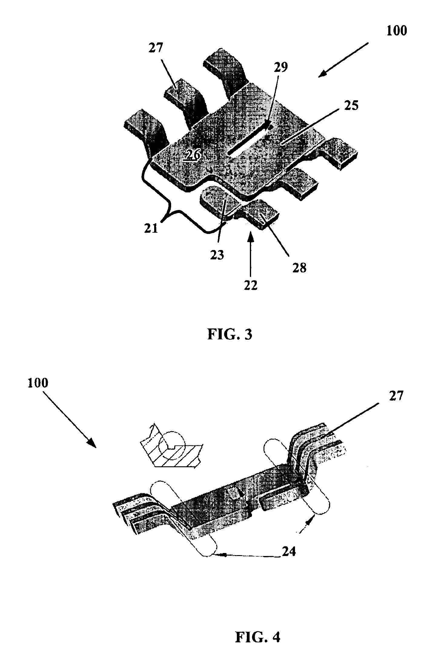
[0009]The invention provides a packaging assembly for semiconductor devices and a method for making such packaging. The invention provides a non-Pb bump design during a new flip-chip method of packaging. The design uses special conductive materials in a stud form, rather than a solder ball containing Pb. This configuration maintains a desirable solder thickness between the die and the leadframe and forms a high standoff by restricting solder wettabilty on the leadframe side. This configuration also absorbs any stress and protects the die from cracking. The invention also provides methods for making such semiconductor packages.
Problems solved by technology
First, because there is a substantially direct electrical connection between the back side of the semiconductor die and the circuit substrate.
When mass producing semiconductor packages of the type described above, a number of problems can occur.
The problems include, for example, silicon cracks that form because of an uneven die standoff from the die attach region of the leadframe structure; moisture seepage into the semiconductor package; delamination between the leadframe structure and the molding material; and finally molding material bleed on an exposed die surface and leads (that can hinder the package from functioning efficiently or potentially fail during device applications).
Other problems include poor solder adhesion between the circuit board bonding pads and the semiconductor die, as well as uneven cutting during the singulation process.
However, Pb is an undesirable material to be used in bumps for two reasons.
First, it is a hazardous material.
Second, the existing electroplated Pb-based solder bumping process is relatively expensive when compared to direct metal bumping processes.
Method used
View moreImage
Smart ImageViewing Examples

Examples
example 1
[0057]The advantages of the invention can also be seen in FIGS. 11-13.
Login to View More PUM
 Abstract
A packaging assembly for semiconductor devices and a method for making such packaging is described. The invention provides a non-Pb bump design during a new flip-chip method of packaging. The design uses special conductive materials in a stud form, rather than a solder ball containing Pb. This configuration maintains a desirable solder thickness between the die and the leadframe and forms a high standoff by restricting solder wettabilty on the leadframe side. This configuration also absorbs any stress and protects the die from cracking. The invention also provides methods for making such semiconductor packages.
Description
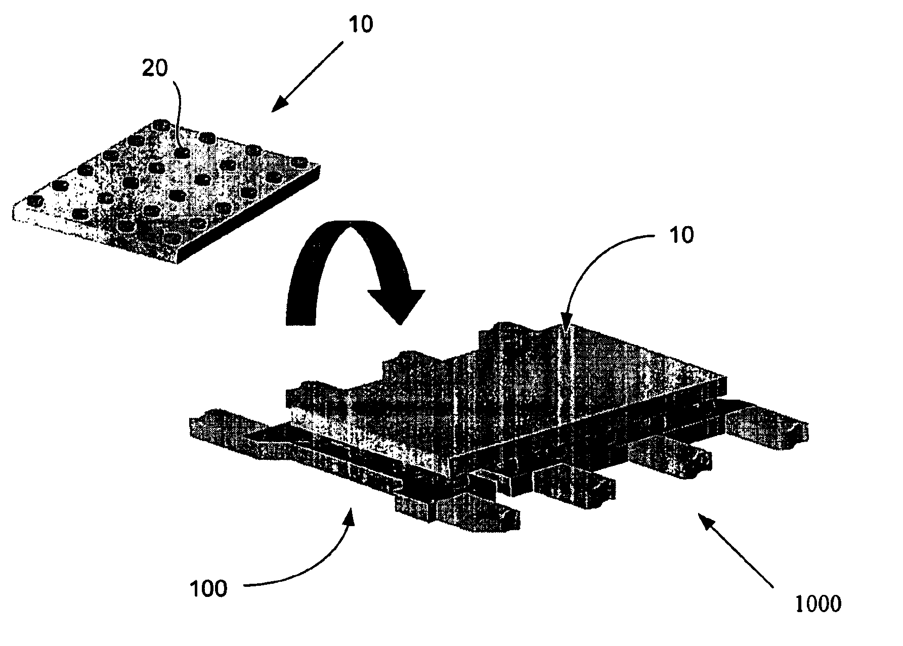
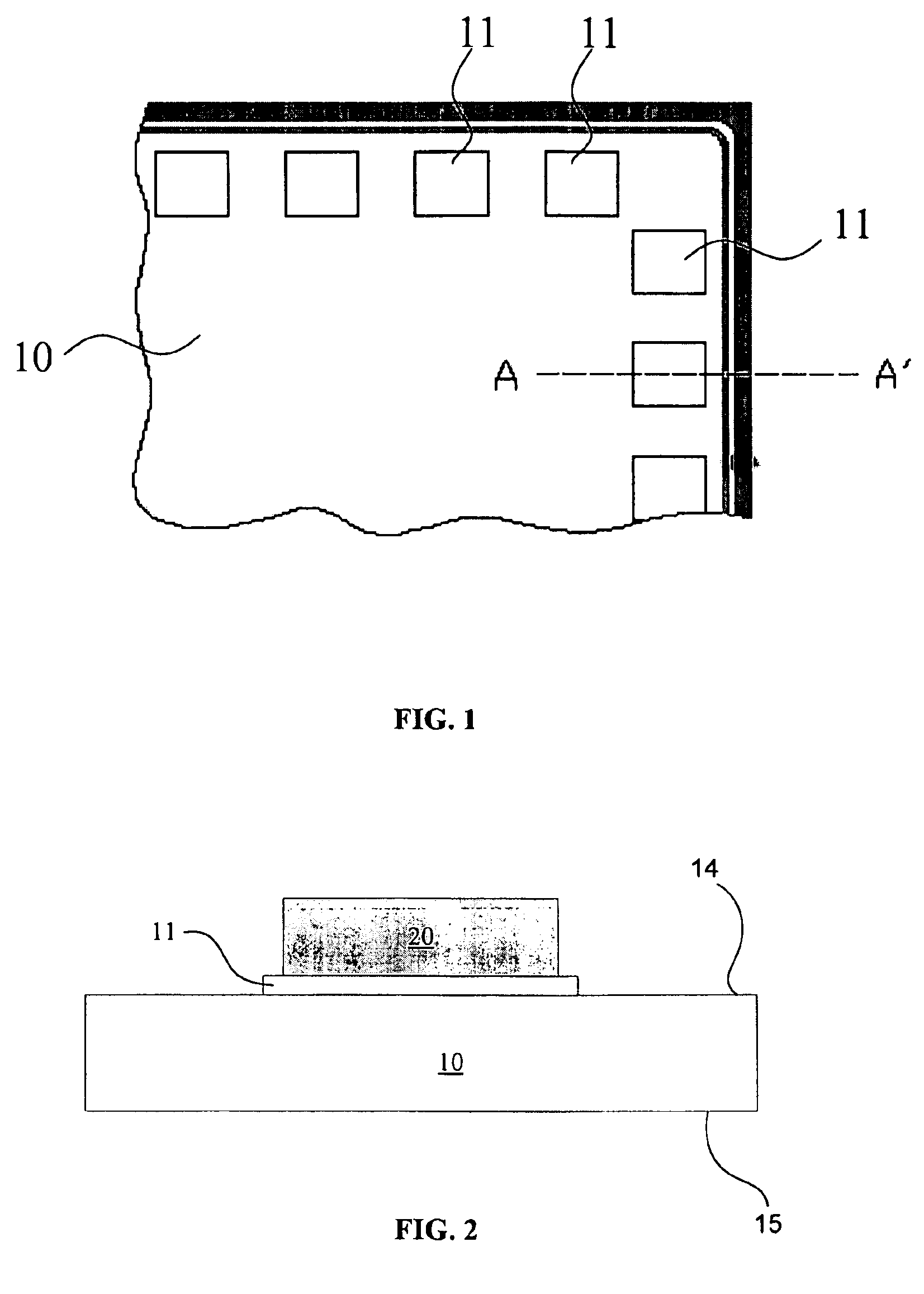
CROSS-REFERENCE TO RELATED APPLICATION[0001]This application claims priority of U.S. Provisional Application No. 60 / 417,800, filed on Oct. 3, 2002, the entire disclosure of which is incorporated by reference.FIELD OF THE INVENTION[0002]The invention generally relates to methods for fabricating integrated circuits (ICs) and semiconductor devices and the resulting structures. More particularly, the invention relates generally to the packaging used for semiconductor devices and methods for making such packaging.BACKGROUND OF THE INVENTION[0003]Semiconductor processing builds hundreds of individual IC chips on a wafer. These individual chips are then cut, tested, assembled, and packaged for their various uses. The packaging step in this processing can be an important step in terms of costs and reliability. The individual IC chip must be connected properly to the external circuitry and packaged in a way that is convenient for use in a larger electrical circuit or system.[0004]There are a...
Claims
Login to View More Application Information
Patent Timeline
 IPC IPC(8): H01L23/48H01L23/495H01L23/485H01L23/31H01L23/28H01L21/60H01L23/544
CPCH01L23/49582H01L23/49586H01L23/544H01L24/10H01L24/81H01L23/49562H01L24/13H01L23/3107H01L2924/1461H01L2223/54473H01L2223/54486H01L2224/13099H01L2224/13144H01L2224/13147H01L2224/16H01L2224/81801H01L2924/01015H01L2924/01027H01L2924/01029H01L2924/01046H01L2924/01058H01L2924/01075H01L2924/01078H01L2924/01079H01L2924/01082H01L2924/13091H01L2924/14H01L2924/18161H01L2924/18301H01L2924/30107H01L2924/00014H01L2924/01005H01L2924/01006H01L2924/01024H01L2924/01033H01L2924/01047H01L2924/014H01L2924/1306H01L2924/10253H01L2224/45099H01L2924/00H01L2924/15747H01L2924/351H01L2924/181H01L2224/1134H01L2924/00013H01L2924/12042H01L2224/13H01L2224/05573H01L2224/05568H01L2224/06135H01L23/3142H01L2224/81205H01L2224/05599
InventorTANGPUZ, CONSUELO N.MANATAD, ROMEL N.RIOS, MARGIE T.CRUZ, ERWIN VICTOR R.
OwnerSEMICON COMPONENTS IND LLC