Semiconductor device having bridge-connected wiring structure

a technology of semiconductor devices and wiring structures, applied in semiconductor devices, solid-state devices, basic electric elements, etc., can solve the problems of increasing loss at semiconductor switches, affecting the operation of semiconductor switches, so as to reduce heat generation, reduce the voltage applied, and reduce the withstand voltage

Inactive Publication Date: 2005-09-13
HITACHI LTD
View PDF10 Cites 33 Cited by
  • Summary
  • Abstract
  • Description
  • Claims
  • Application Information

AI Technical Summary

Benefits of technology

[0014]Meanwhile, the implementation of low-inductance wiring mounting with a small wiring area is becoming increasingly important to the demand for a substantial current increase and a size reduction of a recent semiconductor device. To this end, the conventional example shown in FIG. 4 has been discussed. As a result of its discussions, the following were found. When the amount of current flowing through the wiring for bridge-connecting the semiconductor switches changes, an eddy current opposite to the current path flows in the radiating plate 7. Therefore, the conventional example brings about the effect of reducing the inductance of the wiring for bridge-connecting the semiconductor switches if the radiating plate 7 is made of a material such as copper, AlSiC or the like relatively good in electrical conductivity. This effect results from the fact that mutual inductance caused between the current flowing through the wiring for bridge-connecting the semiconductor switches and its opposed current reduces self-inductance generated in the wiring for bridge-connecting the semiconductor switches. Also this effect has a limit due to the fact that while the current flowing through the wiring for bridge-connecting the semiconductor switches and its opposite current come close to each other and increase to such an extent as to be equal in amount, the wiring for bridge-connecting the semiconductor switches and the radiating plate 7 are spaced away from each other, and the opposite eddy current becomes a small value due to the resistance of the radiating plate 7 as compared with the amount of the current flowing through the wiring for bridge-connecting the semiconductor switches.
[0016]In view of the foregoing, an objective of the present invention is to provide a semiconductor device which reduces the inductance of wiring for bridge-connecting semiconductor switches and realizes a reduction in size.
[0020]According to the present invention, the semiconductor device has a wiring layout at low inductance in the insulating substrate obtained by laminating the conductor boards constituting the current path. It is therefore possible to suppress the voltage applied to the corresponding semiconductor switch at switching and use a semiconductor element of a lower withstand voltage. As a result, the semiconductor device has the effect of reducing heat generated therein.
[0021]In addition, the reduction in inductance brings about the effect of reducing a loss of the semiconductor element at switching. Also the reduction in the generated heat is effective in improving reliability and in reducing cooling cost.
[0022]According to the present invention, the area of an insulating substrate portion is reduced. Therefore, the present invention is effective even in reducing the semiconductor device in size. Owing to the effect, a power converter can be provided using a semiconductor device which realizes a significant increase in current and a reduction in size.

Problems solved by technology

When the pop-up voltage increases and the voltage applied to the corresponding semiconductor switch switched from on to off exceeds a device withstand voltage, an electrical breakdown occurs.
When, however, the withstand voltage is increased, the semiconductor switch has a tendency that the resistance value in its on-state becomes large.
Particularly, a system in which a power supply voltage is low and a large current flows in each semiconductor switch causes a problem that a loss at the semiconductor switch increases.

Method used


Image

  • Semiconductor device having bridge-connected wiring structure
  • Semiconductor device having bridge-connected wiring structure
  • Semiconductor device having bridge-connected wiring structure

Examples


first embodiment

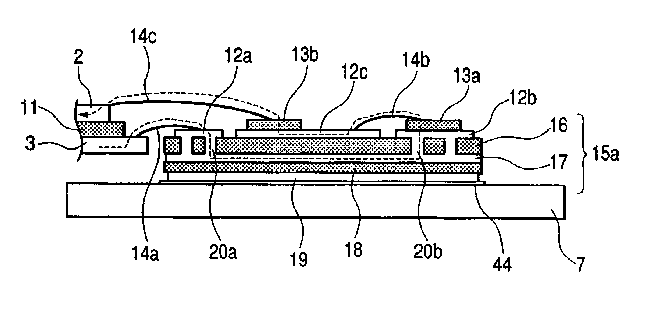
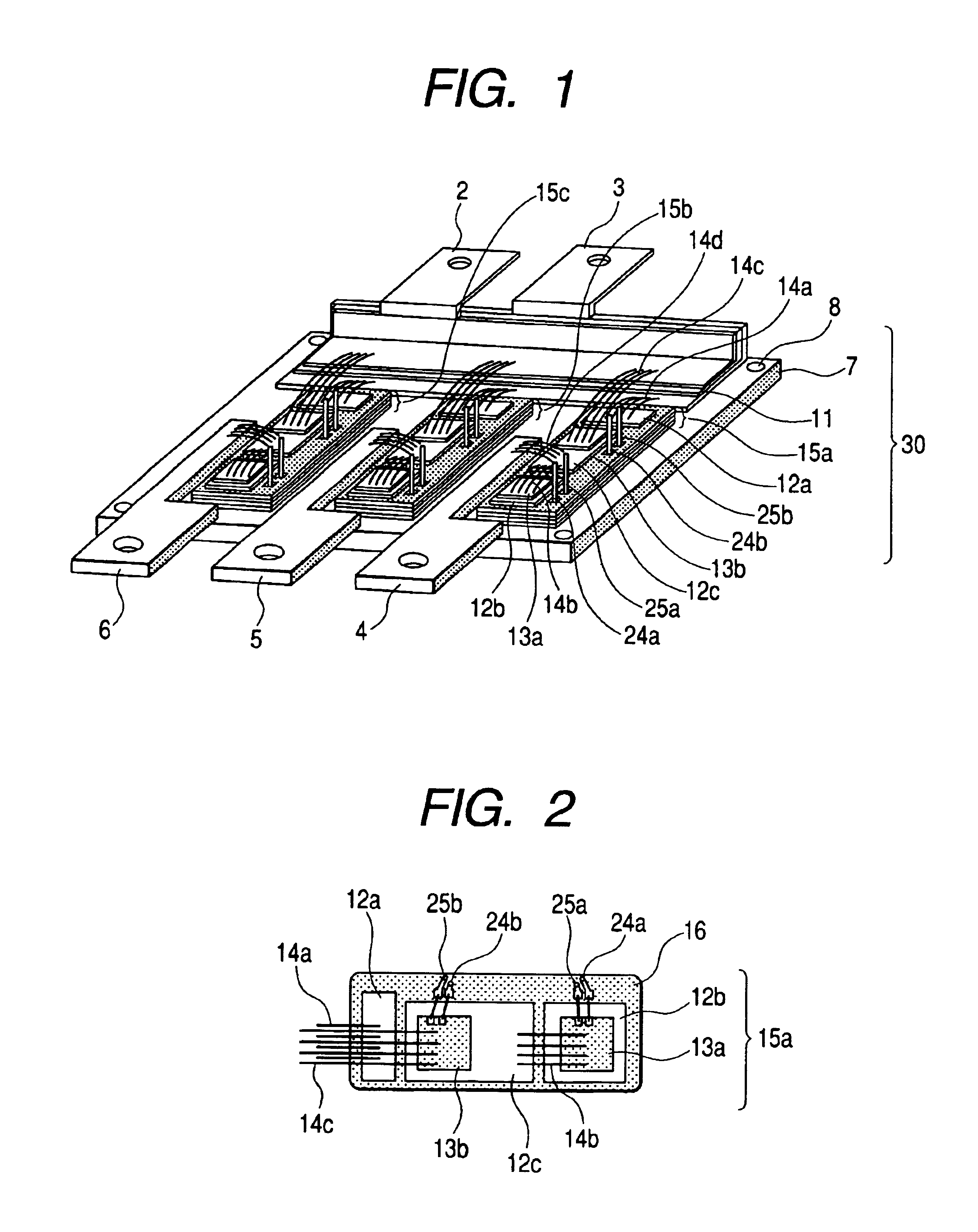
[0040]FIG. 1 is a general view showing a wiring structure of a semiconductor device according to the present invention. In FIG. 1, a semiconductor device 30 is shown. Reference numeral 2 designates a negative polarity DC terminal, 3 designates a positive polarity DC terminal, 4, 5 and 6 designate output terminals and a wiring board, 7 designates a radiating plate, 8 designate threaded holes, and 11 designates an insulating board. In addition, reference numerals 12a, 12b and 12c designate substrate conductor patterns, 13a and 13b designate diode and semiconductor switches, 14a, 14b, 14c and 14d designate wire interconnections, 15a, 15b and 15c designate insulating boards or substrates, 24a and 24b designate gate signal terminals, and 25a and 25b designate ground terminals. The respective terminals 2, 3, 4, 5 and 6 are provided with wiring mounting holes. The threaded holes 8 are used when a cooling fin and the radiating plate 7 are fixed with bolts or the like.

[0041]Although the wire...

second embodiment

[0063]A description will next be made of a wiring layout for increasing the longevity of solder joining between semiconductor switches and substrate conductor patterns employed in a semiconductor device according to the present invention, with reference to FIGS. 8 and 9. FIG. 8 is a perspective view showing a wiring structure of the semiconductor device according to the present embodiment, with a case portion of the semiconductor device omitted in drawing.

[0064]In FIG. 8, reference numeral 30 designates the semiconductor device, reference numeral 2 designates a negative polarity DC terminal, 3 designates a positive polarity DC terminal, 4, 5 and 6 designate output terminals and a wiring board, 7 designates a radiating plate, reference numerals 8 designate threaded holes, 11 designates an insulating board, 12a, 12b, 12c and 12d designate substrate conductor patterns, 13a and 13b designate diode and semiconductor switches, 14a, 14b, 14c, 14d and 14e designate wire interconnections, 15...

third embodiment

[0077]A semiconductor device according to the present invention, wherein semiconductor switches are arranged in parallel, will next be explained with reference to FIGS. 10 and 11. FIG. 10 is a plan view of the semiconductor device employed in the present embodiment with the semiconductor switches arranged in a two parallel form. In FIG. 10, the upper surface portion of a case of the semiconductor device has been omitted from FIG. 10 to show an internal wiring structure.

[0078]In FIG. 10, reference numeral 30 designates a semiconductor device, reference numeral 2 designates a negative polarity DC terminal, 3 designates a positive polarity DC terminal, 4, 5 and 6 designate output terminals and a wiring board, 13a, 13b, 13c and 13d designate diode and semiconductor switches, 14b and 14e designate wire interconnections, 15a, 15b and 15c designate insulating substrates, 24a and 24b designate gate signal terminals, 25a and 25b designate ground terminals, 27a and 27b designate drain signal ...


PUM


Abstract

The present invention provides a semiconductor device which reduces an inductance of wiring for bridge-connecting semiconductor switches and realizes a reduction in size. Within the semiconductor device formed are two controllable bridge-connected semiconductor switches 13a and 13b, an output terminal, positive / negative polarity DC terminals 2 and 3, and an insulating substrate 15a in which conductor layers 12, 17 and 19 having a conductor section and in an inner layer for bridge-connecting the semiconductor switches to the DC terminals on a surface thereof and insulating layers 16 and 18 are alternately laminated. The surface and inner-layer conductor layers 12 and 17 which interpose the insulating layer 16 therebetween are electrically connected by a conductor 20 passing through the insulating layer 16 interposed between the conductor layers 12 and 17. A current path (dotted line) is so provided as to allow current flowing through a bridge circuit for mounting the two semiconductor switches on the insulating substrate to flow in opposite directions between the conductor layers 12 and 17 which interpose the insulating layer 16 therebetween.

Description

TECHNICAL FIELD[0001]The present invention relates to a semiconductor device, and particularly to a technology for reducing wiring inductance that leads to an increase in loss at switching and the occurrence of a pop-up voltage.BACKGROUND ART[0002]As a prior art, a technology for reducing inductance that leads to a pop-up voltage in a power converter using a semiconductor device has been disclosed in Japanese Patent Laid-open No. 11-89247. The prior technology is a method that reduces the inductance of wiring for connecting the semiconductor device and the capacitors with a conductor board laminated by interposing an insulator between the semiconductor device and the capacitors. Thereby the wiring inductance that leads to an increase in loss at switching and the occurrence of a pop-up voltage is reduced.[0003]Now a necessary minimum circuit composition of the power converter will be explained with reference of FIG. 6. In FIG. 6, the power converter 32 comprises a semiconductor devic...

Claims


Application Information

Patent Timeline
Patent Type & Authority Patents(United States)
IPC IPC(8): H01L23/538H01L23/52H01L25/07H02M7/00
CPCH01L23/5383H02M7/003H01L24/49H01L25/072H01L25/18H01L23/645H01L2924/1305H01L2924/19107H01L2224/48227H01L2224/32225H01L2224/73265H01L2924/014H01L2924/01023H01L24/48H01L2924/30107H01L2924/30105H01L2924/19043H01L2924/19041H01L2924/13091H01L2924/13055H01L2924/01082H01L2924/01074H01L2924/01033H01L2924/01029H01L2924/01014H01L2924/01013H01L2924/01006H01L2224/48091H01L2224/48472H01L2224/49111H01L2224/49175H01L2924/01005H01L2924/00014H01L2924/00H01L2924/00012H01L2224/48111H01L2224/40225H01L2224/49431H01L2224/49433H01L2224/0603H01L2224/73221H01L2224/45099H01L2224/05599
Inventor SHIRAKAWA, SHINJIMISHIMA, AKIRAMASHINO, KEIICHIINNAMI, TOSHIYUKIFUJINO, SHINICHIANAN, HIROMICHIOCHIAI, YOSHITAKA
Owner HITACHI LTD
Why Eureka
Try Eureka