Capacitor and method for fabricating the same

a technology of capacitors and capacitors, applied in the field of capacitors, can solve the problems of deterioration of cell critical dimension, short circuit between cylinders, and inability to apply the above method in practice,

Inactive Publication Date: 2005-09-20
SK HYNIX INC
View PDF24 Cites 4 Cited by
  • Summary
  • Abstract
  • Description
  • Claims
  • Application Information

AI Technical Summary

Benefits of technology

[0015]It is, therefore, an object of the present invention to provide a method for manufacturing a capacitor in a semiconductor device for securing capacitance without a merging phenomenon during a MPS grain growth process.

Problems solved by technology

However, in the cylinder typed capacitor in which the MPS grains are formed on inner walls and outer walls of electrodes, there is a drawback that a bridge between each neighboring cylinders is happened due to the MPS grains formed on outer walls of the electrodes, thereby causing an electrical-short phenomenon between each cylinder.
But, since a critical dimension between neighboring cells is reduced sharply, it is impossible to apply the above method in practice.
Therefore, a cell critical dimension may be deteriorated because the top critical dimension is larger than the bottom critical dimension.
The merging phenomenon gives rise to a serious problem that a step coverage of the dielectric layer such as tantalum oxide becomes deteriorated.
Furthermore, an electric field is concentrated during the operation of the device so that leakage current may be increased, thereby inducing the decrease of a breakdown voltage eventually.

Method used


Image

  • Capacitor and method for fabricating the same
  • Capacitor and method for fabricating the same
  • Capacitor and method for fabricating the same

Examples


first embodiment

[0031]In accordance with the present invention, the MPS grains 40 are formed on a sidewall of the inner wall of the first electrode 38 except a bottom region, thereby securing capacitance of the capacitor sufficiently.

[0032]Referring to FIGS. 3A to 3G, there are shown cross sectional views illustrating a method for manufacturing a capacitor in accordance with a first preferred embodiment of the present invention.

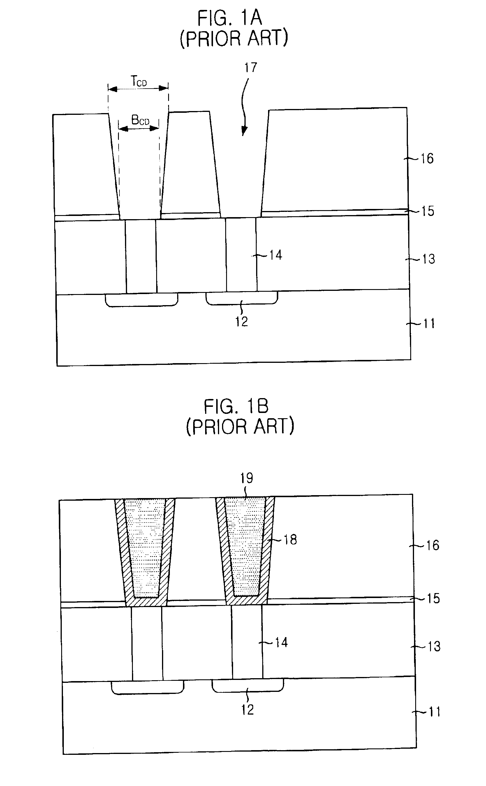
[0033]Referring to FIG. 3A, the manufacturing process begins with preparation of a semiconductor substrate 31 having a conductive region 32 doped with impurities, i.e., source / drain region.

[0034]Thereafter, an ILD layer 33 is formed on the top face of the semiconductor substrate 31 and is patterned into a predetermined configuration by using a contact mask to form a contact hole till the contact hole is completely filled in. Next, a conductive layer is deposited on entire surface including the contact hole. Subsequently, a contact plug 34 is formed by using a technique such ...

second embodiment

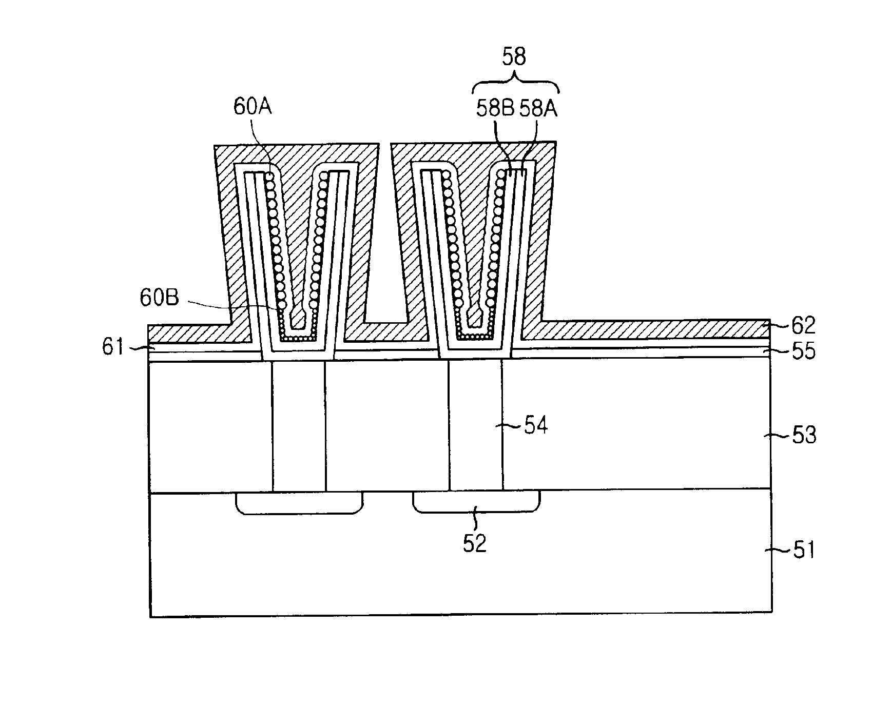
[0052]In accordance with the present invention, the first electrode 58 includes the first region and the second region, wherein the first region has the second MPS grains 60B that are small enough to prevent the merging phenomenon and the second region has the first MPS grains 60A that are larger than those of the second MPS grains 60B. Therefore, it is possible to obtain a sufficient capacitance. Namely, the increment ratio of the cross section area of the first region is lower than that of the second region, wherein the increment ratio of the cross section area of the first region ranges from approximately 1.1 to approximately 1.5 and the increment ratio of the cross section area of the second region ranges from approximately 1.7 to approximately 2.0. Additionally, the second MPS grains 60B formed in the bottom area of the first electrode 58 are small enough to prevent the merging phenomenon, thereby having good step coverage of the dielectric layer 61.

[0053]Referring to FIGS. 5A ...


PUM

PropertyMeasurementUnit
capacitanceaaaaaaaaaa
dielectric constantaaaaaaaaaa

Abstract

A method for manufacturing a capacitor in a semiconductor device for securing capacitance without a merging phenomenon during a MPS grain growth process. The manufacturing step begins with a preparation of a substrate. The interlayer dielectric (ILD) layer is formed on the substrate and is etched to form conductive plug. Then, an etch barrier layer and a sacrifice insulating layer are formed on entire surface subsequently. A cylinder typed first electrode is formed over the conductive plug using the sacrifice insulating layer. Thereafter, first meta-stable poly silicon (MPS) grains are formed on inner wall of the first electrode except a bottom region thereof. However, second MPS grains with small sizes can be formed in the bottom region for increasing a storage area of the first electrode. Finally, a dielectric layer and a second electrode are formed on the first electrode subsequently.

Description

FIELD OF THE INVENTION[0001]The present invention relates to a semiconductor device; and, more particularly, to a capacitor in the semiconductor device and a method for manufacturing the same, for preventing merging phenomenon of meta-stable poly silicon (MPS) grains having a good step coverage of a dielectric layer.DESCRIPTION OF THE PRIOR ART[0002]In recent years, several researches are advanced for securing a capacitance of about 25 fF to be required in a cell in spite of decreasing a minimum line width of a dynamic random access memory (DRAM) device and a high-density integrated circuit.[0003]Generally, in order to secure the capacitance, there are two kinds of methods to be researched. One is to develop a dielectric material with a high dielectric constant and the other is to develop a structure of the cell capacitor. Therefore, there has been proposed the capacitor having a high dielectric material or a new structure for increasing a surface of a charge storage electrode, such...

Claims


Application Information

Patent Timeline
Patent Type & Authority Patents(United States)
IPC IPC(8): H01L21/02H01L21/8242H01L27/108
CPCH01L27/10817H01L28/84H01L27/10852H01L28/90H10B12/318H10B12/033H10B99/00
Inventor SHIN, DONG-WOOCHOI, HYUNG-BOK
Owner SK HYNIX INC
Why Eureka
Try Eureka