Light emitting semiconductor method and device

a technology of semiconductors and semiconductor devices, applied in semiconductor devices, semiconductor/solid-state device details, electrical devices, etc., can solve problems such as degrading device efficiency

Inactive Publication Date: 2005-09-20
LUMILEDS
View PDF26 Cites 55 Cited by
  • Summary
  • Abstract
  • Description
  • Claims
  • Application Information

AI Technical Summary

Benefits of technology

[0012]In accordance with a form of the invention, there is defined a light-emitting device which comprises a semiconductor structure having a plurality of semiconductor layers and including an active region within the layers. First and second conductive metal electrodes contact respectively different semiconductor layers of the structure. A migration barrier is provided for preventing migration of metal from at least one of said electrodes onto the surface of the semiconductor layer with which said at least one electrode is in contact.
[0013]In one preferred embodiment of the invention, there is defined a

Problems solved by technology

Electrochemical migration of the silver metallization to the pn junction of the device resu

Method used


Image

  • Light emitting semiconductor method and device
  • Light emitting semiconductor method and device
  • Light emitting semiconductor method and device

Examples


Embodiment Construction

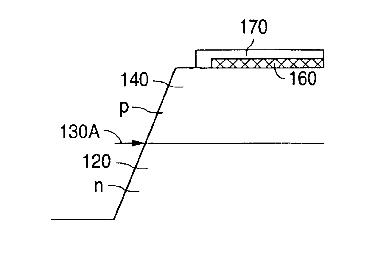
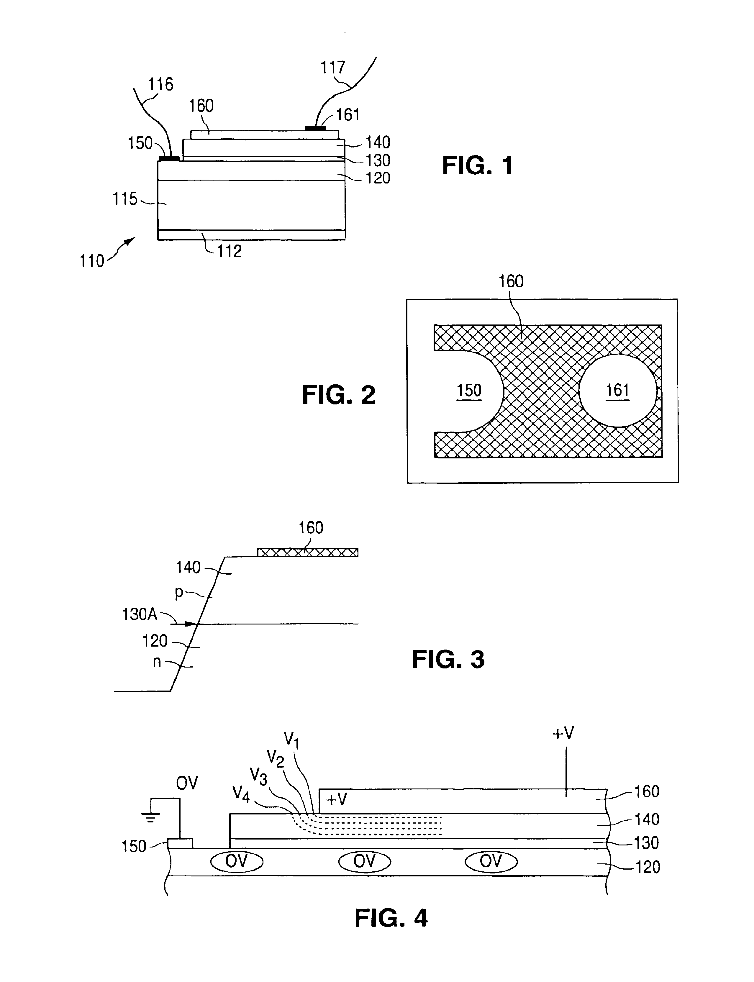
[0031]FIG. 1 illustrates a III-V nitride light emitting diode (LED) 110 that includes a bottom reflective layer 112, a substrate 115, which may be for example a sapphire, SiC, or GaN substrate, an n-type layer 120 of a III-V nitride semiconductor for example n-type GaN, and a p-type layer 140 of a III-V nitride semiconductor for example p-type GaN. The active region 130 can be the p-n junction itself or, more typically, a single quantum well or multiple quantum wells of III-V nitride between barrier layers of another III-V nitride, for example using InGaN and AlGaN. It will be understood that any suitable III-V nitride semiconductors can be used for any of the semiconductor layers of the device, and that suitable additional semiconductor layers can be employed in the device. A conductive metal electrode 150 (the n-electrode) is deposited on the n-type layer 120 and a conductive metal electrode 160 (the p-electrode) is deposited on the p-type layer 140. As first noted above, the p-el...


PUM


Abstract

Silver electrode metallization in light emitting devices is subject to electrochemical migration in the presence of moisture and an electric field. Electrochemical migration of the silver metallization to the pn junction of the device results in an alternate shunt path across the junction, which degrades efficiency of the device. In accordance with a form of this invention, a migration barrier is provided for preventing migration of metal from at least one of the electrodes onto the surface of the semiconductor layer with which the electrode is in contact.

Description

RELATED APPLICATION[0001]The subject matter of this application is generally related to subject matter disclosed in copending U.S. patent application Ser. No. 09 / 652,544, filed of even date herewith and assigned to the same assignee as the present application.FIELD OF THE INVENTION[0002]This invention relates to light emitting semiconductor structures and methods of making same and, more particularly, to devices and methods employing III-V nitride semiconductors and to improving the operation thereof.BACKGROUND OF THE INVENTION[0003]Light emitting semiconductors which emit in several regions of the visible spectrum, for example group III-V semiconductors such as aluminum gallium arsenide and gallium phosphide, have achieved commercial acceptance for various applications. However, for applications which require blue or green light, for example green to be used for traffic signal lights or blue for a component of a red-green-blue primary color combination to be used for white lighting...

Claims


Application Information

Patent Timeline
IPC IPC(8): H01L29/02H01L29/22H01L33/32H01L33/40
CPCH01L33/405H01L33/32H01L2224/49107
Inventor STEIGERWALD, DANIEL A.LUDOWISE, MICHAEL J.MARANOWSKI, STEVEN A.RUDAZ, SERGE L.BHAT, JEROME C.
Owner LUMILEDS
Why Eureka
Try Eureka