Method of fabricating a semiconductor multilevel interconnect structure

a multi-level interconnect and semiconductor technology, applied in the field of semiconductor memory and logic devices, can solve the problems of structural defects in the via, adversely affecting the performance of the multi-level interconnect, and poisoning of the imd, and achieve the effect of reducing the above-described deficiencies

Inactive Publication Date: 2005-10-04
MICRON TECH INC
View PDF4 Cites 35 Cited by
  • Summary
  • Abstract
  • Description
  • Claims
  • Application Information

AI Technical Summary

Benefits of technology

[0013]The present invention provides a method of fabricating a semiconductor multilevel interconnect structure, as well as the resulting structure. More specifically, the present invention provides a dual damascene method of fabrication using a dual hardmask technique that mitigates the above-described deficiencies associated with conventional processes.
[0014]Accordingly, the present invention relates to a dual damascene, dual hardmask, method of fabrication using amorphous carbon as a first hardmask layer capable of being etched by a second etch process, and a second hardmask layer capable of being etched by a first etch process. By virtue of the selective etch chemistry employed with the dual hardmask, the present method affords flexibility unattainable with conventional dual damascene processes.
[0017]The present method and structure have several advantages over conventional dual damascene processes and structures. First, by virtue of the protective layers, the via, after being opened, is never in contact with the photoresist. This eliminates the “ear” formation problem at the trench / via edge which results from the presence of photoresist residue on the IMD layer.
[0018]Secondly, this processing sequence eliminates the potential “poisoning” of the IMD layer which can result from the interaction between the photoresist and the IMD layer during application of the photoresist.
[0019]Thirdly, the photolithographic imaging for both the trench and the via are completed before the IMD etch, so, if necessary, it is easy to rework any patterning misalignments to ensure that both the trench and the via are etched correctly.

Problems solved by technology

Despite the benefits of using interconnects such as those fabricated from copper, there can be certain drawbacks associated with use of a conventional dual damascene process.
First, the conventional process can leave an undesirable “ear” (or “fence” or “fender”) formation of photoresist residue at the trench / via edge. FIG. 6 is a partial cross-sectional view of a structure 300 fabricated by a conventional dual damascene process.
The presence of the photoresist residue can adversely affect the performance of the multilevel interconnect.
Secondly, one of the major problems associated with dual damascene integration, especially when a low k IMD layer is used, is the “poisoning” of the IMD which can result from the interaction between the photoresist and the IMD.
The subsequent outgassing of these chemicals during via metallization leads to structural defects in the via.
Thirdly, another drawback associated with conventional dual damascene processes is their lack of flexibility. For example, with the conventional process, the IMD may be partially etched before the trench and / or via patterning are completed. If there is any misalignment in the trench / via patterning, it cannot be corrected once the IMD has been etched.
That is, because the photoresist must be etch resistant (i.e., relatively thick) in a conventional process, the imaging qualities of the photoresist may be compromised for the benefit of etch performance.

Method used


Image

  • Method of fabricating a semiconductor multilevel interconnect structure
  • Method of fabricating a semiconductor multilevel interconnect structure
  • Method of fabricating a semiconductor multilevel interconnect structure

Examples


Embodiment Construction

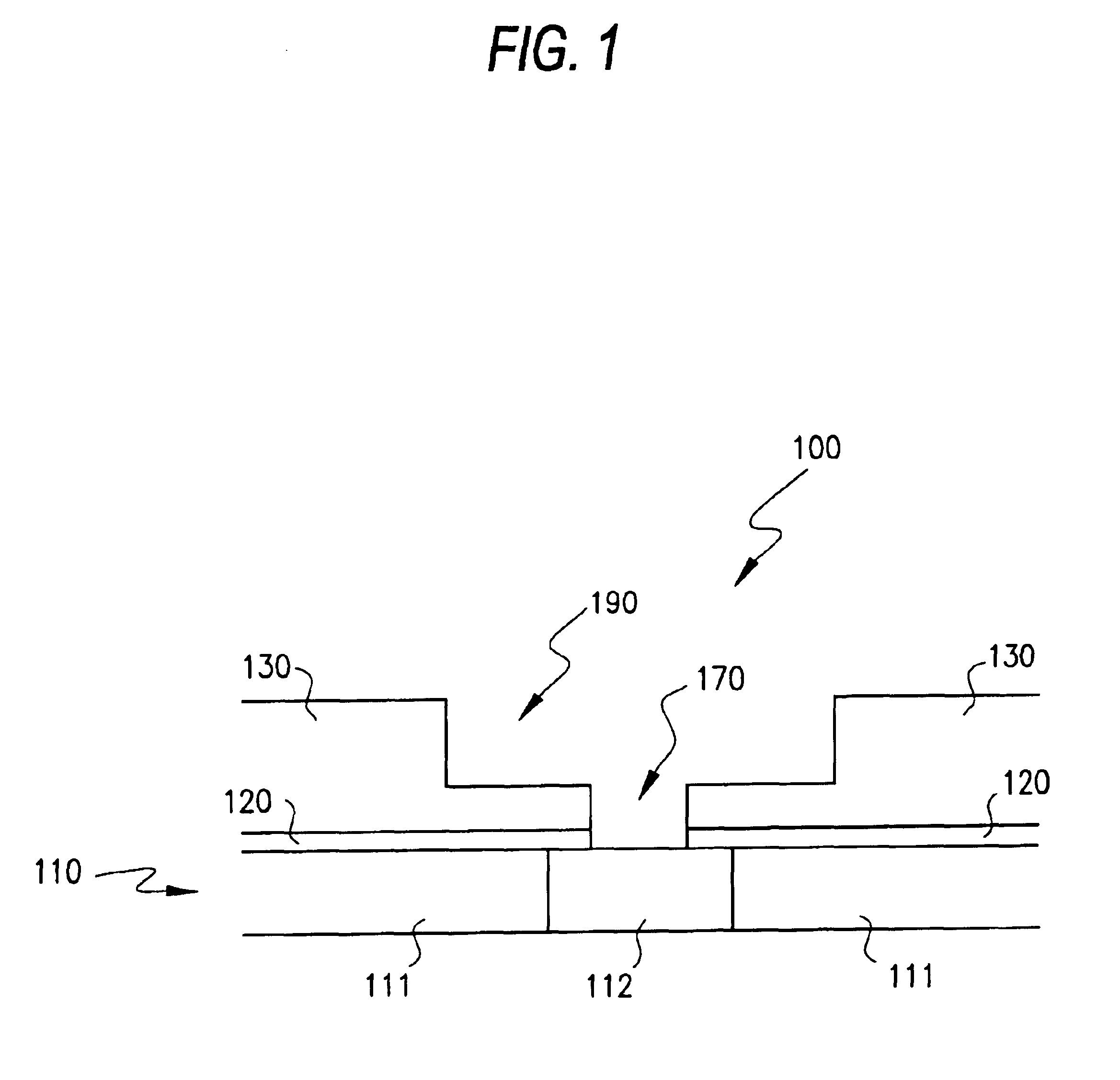
[0028]FIG. 1 is a partial cross-sectional view of an interconnect structure 100 constructed in accordance with the present invention for use with a multilevel interconnect. Structure 100, the fabrication of which is described below, includes a first layer 110 having a first intermetal dielectric layer 111 and a metal portion 112; an etched protective layer 120; an etched second intermetal dielectric layer 130; a via 170; and a trench 190. Structure 100 can accommodate the deposition of an inlaid multilevel interconnect metal. As is evident from FIG. 1, structure 100 is characterized by the absence of any undesirable “ear” (i.e., structural formation of resist residue) on the etched IMD layer 130 at the trench / via edge.

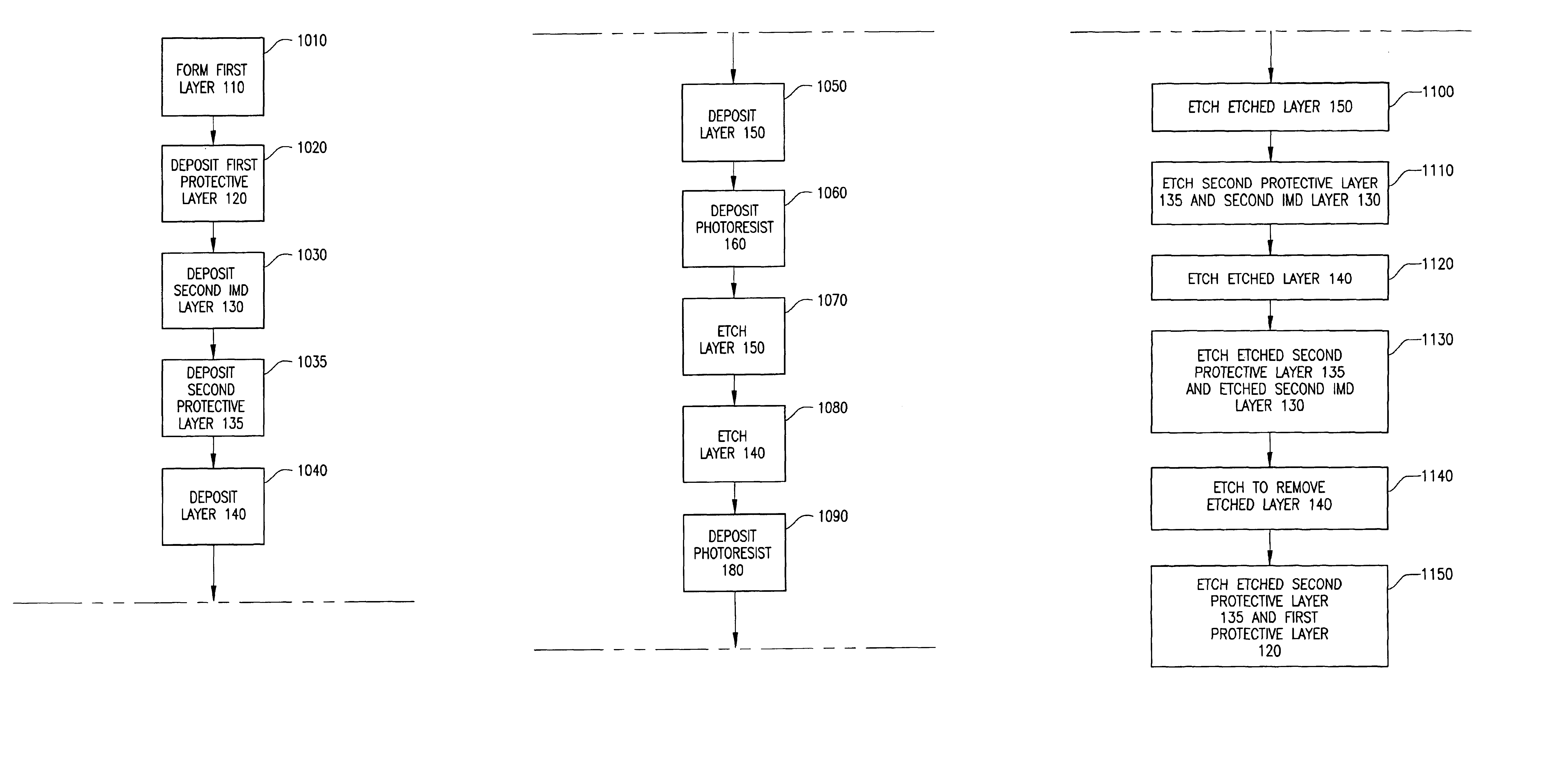
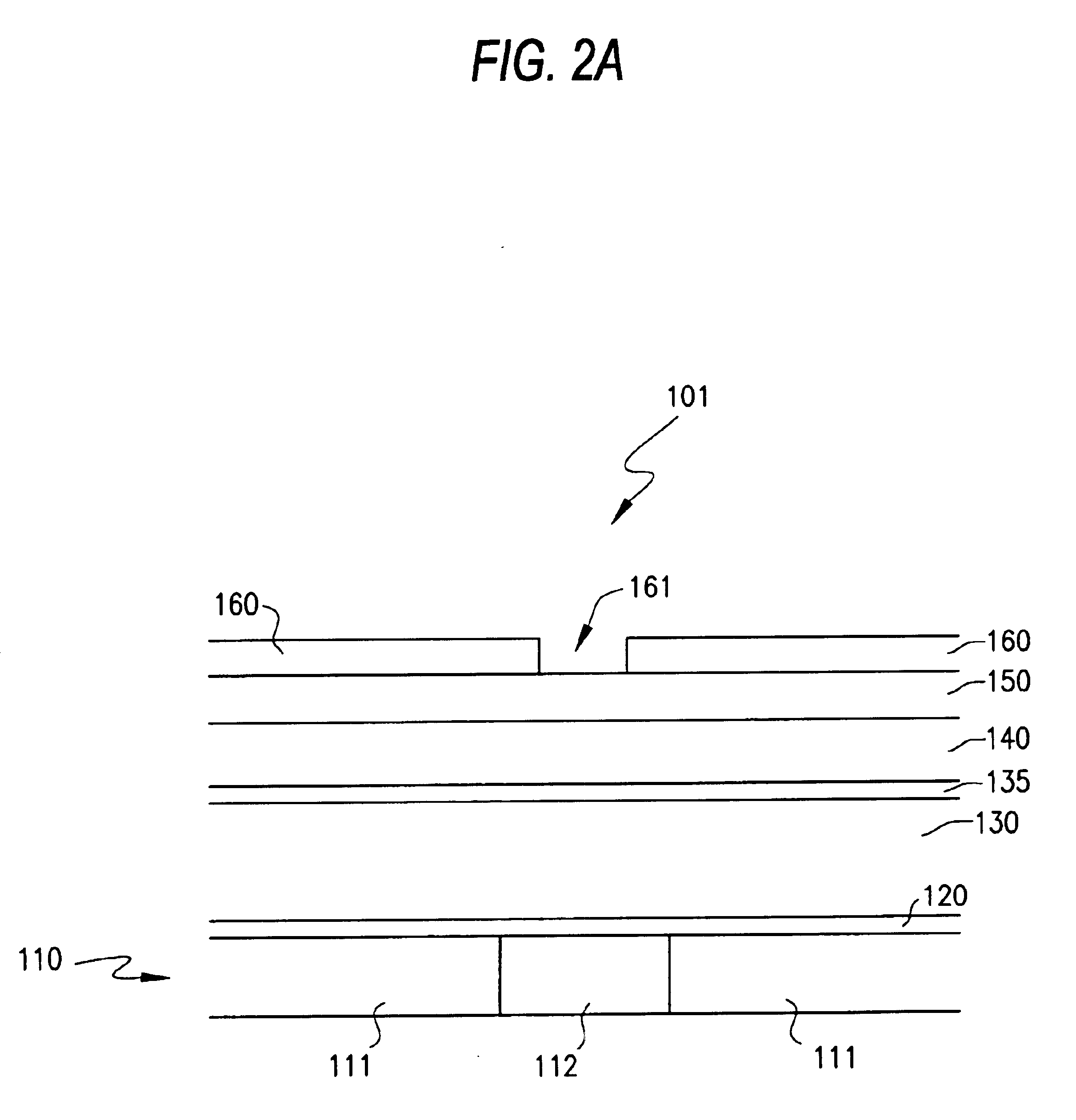
[0029]FIGS. 2A-J illustrate a first embodiment of the method of fabricating the structure 100 depicted in FIG. 1. FIGS. 3A-C are a flow diagram of the fabrication sequence corresponding to FIGS. 2A-J. The method includes first assembling a dual hardmask structure to be...


PUM

PropertyMeasurementUnit
semiconductoraaaaaaaaaa
dielectricaaaaaaaaaa
lengthaaaaaaaaaa

Abstract

A method of fabricating a semiconductor multilevel interconnect structure employs a dual hardmask technique in a dual damascene process. The method includes using amorphous carbon as a first hardmask layer capable of being etched by a second etch process, and a second hardmask layer capable of being etched by a first etch process, as a dual hardmask. By virtue of the selective etch chemistry employed with the dual hardmask, the method affords flexibility unattainable with conventional processes. The via is never in contact with the photoresist, thus eliminating residual photoresist at the trench / via edge and the potential “poisoning” of the intermetal dielectric layer. Since trench / via imaging is completed before further etching, any patterning misalignments can be easily reworked. Because the amorphous carbon layer and the second hardmask layer are used as the dual hardmask, the photoresist can be made thinner and thus optimized for the best imaging performance.

Description

BACKGROUND OF THE INVENTION[0001]1. Field of the Invention[0002]This invention relates generally to the field of semiconductor memory and logic devices. The invention relates more specifically to a method of fabricating a semiconductor multilevel interconnect structure, as well as the resulting structure.[0003]2. Description of the Related Art[0004]In order to improve the speed of semiconductor devices on integrated circuits, it has become desirable to use conductive materials, such as copper, having low resistivity and low k (a dielectric constant of less than 4.0) in order to reduce the capacitive coupling between structures such as interconnect lines.[0005]Because materials such as copper are difficult to etch in a precise pattern, a method of fabrication known as a dual damascene process can be used to form the interconnects. In a conventional dual damascene process, a dielectric layer is etched to define both the contacts and vias, and the interconnect lines. Metal is then inla...

Claims


Application Information

Patent Timeline
Patent Type & Authority Patents(United States)
IPC IPC(8): B32B15/04B32B9/04B32B9/06G03F7/36G03F7/20G03F7/40G03F7/00G03F7/11H01L21/033H01L21/311H01L21/3213H01L21/768
CPCH01L21/0331H01L21/31127H01L21/31144H01L21/32139H01L21/76811
Inventor LI, WEIMIN
Owner MICRON TECH INC
Why Eureka
Try Eureka