Fixed wavelength vertical cavity optical devices and method of manufacture therefor

a technology of optical devices and vertical cavities, applied in the direction of semiconductor laser arrangements, semiconductor laser structure details, semiconductor lasers, etc., can solve the problems of limiting the temperature range of useful performance of vcsels, affecting the production efficiency of vcsels, and increasing the difficulty of producing vcsels

Inactive Publication Date: 2005-10-11
AVAGO TECH WIRELESS IP SINGAPORE PTE
View PDF18 Cites 37 Cited by
  • Summary
  • Abstract
  • Description
  • Claims
  • Application Information

AI Technical Summary

Benefits of technology

[0012]The present invention provides vertical cavity optical devices, and a method of manufacturing therefor, where the method includes partially forming a first vertical cavity optical device on a wafer, adjusting the lasing wavelength of the first vertical cavity optical device, and fixing the lasing wavelength of the first vertical cavity optical device to complete the forming thereof. In this way, the Fabry-Perot resonance and the semiconductor gain-peak can be aligned subsequent to the fabrication of the semiconductor material.

Problems solved by technology

Alignment of the wavelength of maximum gain for the laser gain media and the cavity modes of the laser, set by the optical cavity height of the structure significantly increases the difficulty of producing VCSELs.
This is a big yield problem in VCSEL manufacturing because the optical cavity height is permanently set during the material fabrication process making it impossible to adjust later.
Also, this limits the temperature range of useful performance for VCSELs since the optical cavity height changes with temperature due to the thermal expansion of the laser material.
This presents a problem because the processing used on the wafer must assure that the threshold gain at which lasing begins, the current usage, the efficiency, the losses of light in the resonant cavity, the amplification of the gain material, and the light transmission of the DBR all remain the same.
Solutions to these problems have been long sought but have long eluded those skilled in the art.

Method used


Image

  • Fixed wavelength vertical cavity optical devices and method of manufacture therefor
  • Fixed wavelength vertical cavity optical devices and method of manufacture therefor
  • Fixed wavelength vertical cavity optical devices and method of manufacture therefor

Examples


Embodiment Construction

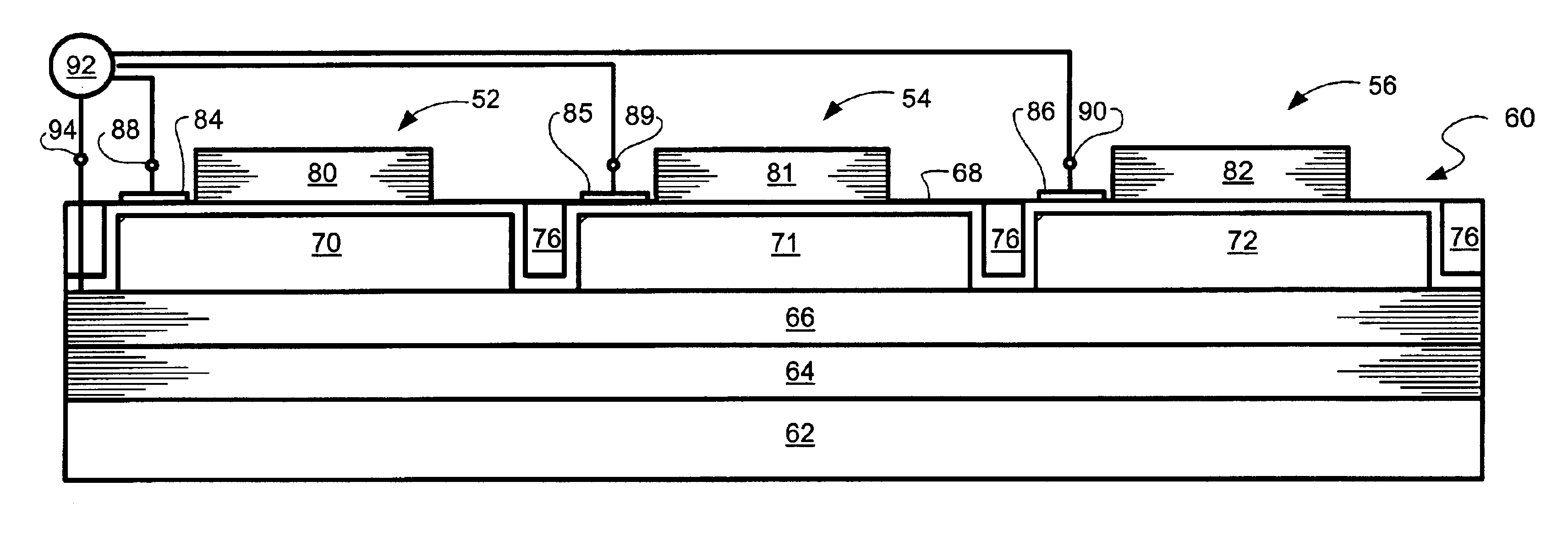
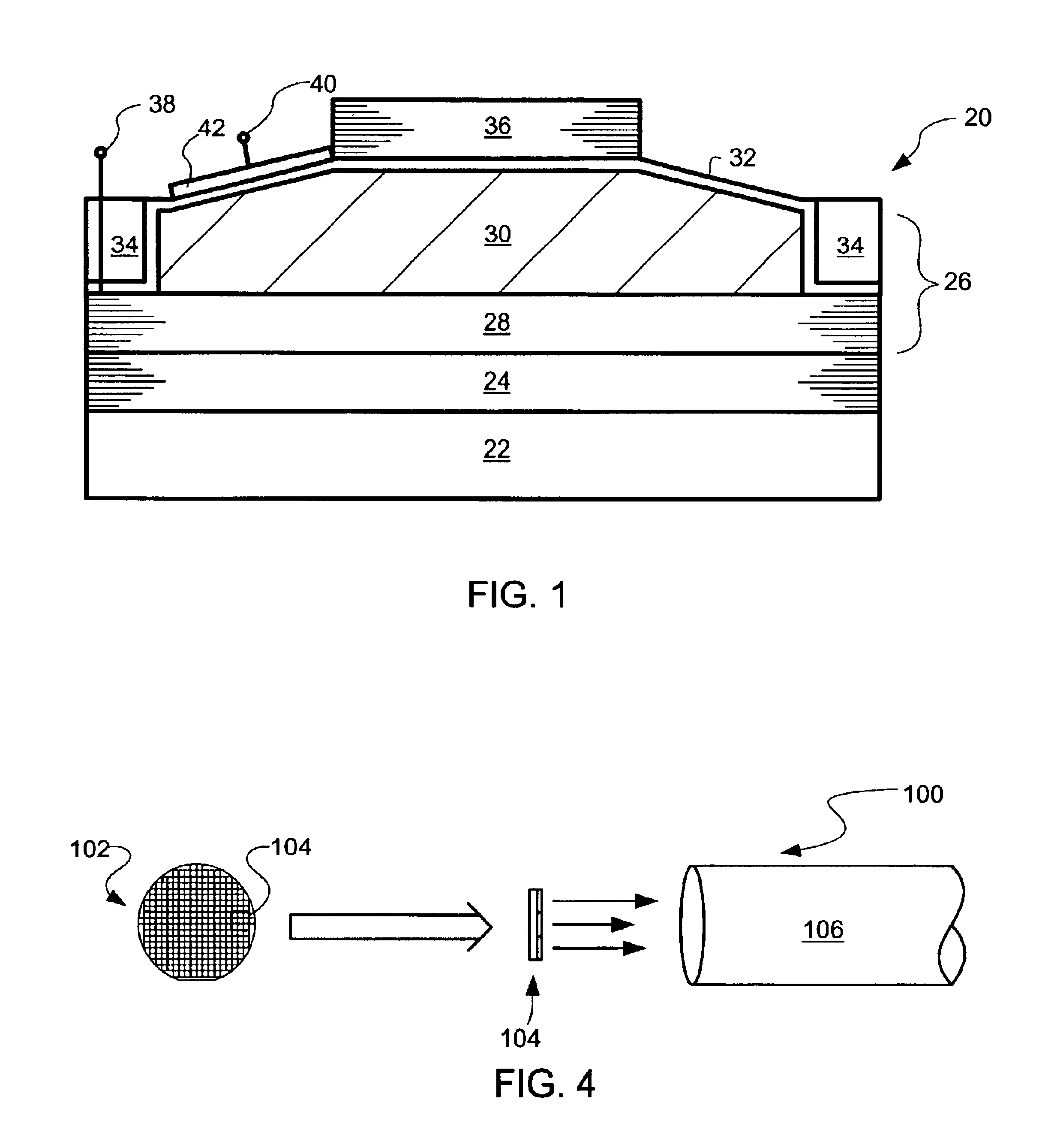
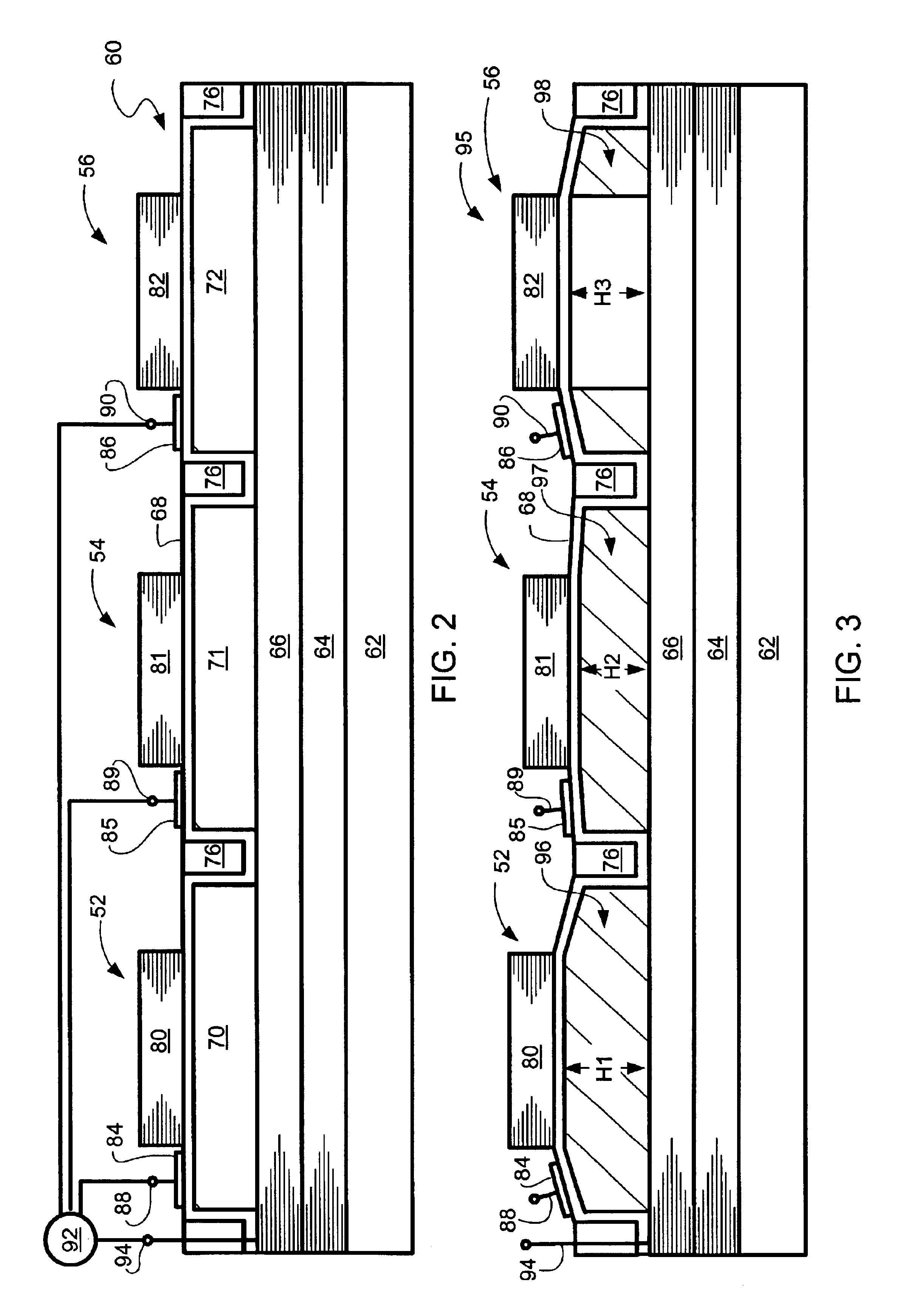
[0019]For purposes of the present invention, the vertical resonant cavity device is referred to as a vertical cavity optical device (VCOD). This is because in addition to VCSELs the invention can also be used to make detectors, Fabry-Perot filters, or other optical devices that require a range of resonant cavity wavelengths.

[0020]In addition, for purposes of convenience, the term “horizontal” as used in herein is defined as a plane parallel to the conventional plane or surface of a wafer upon which the VCODs are formed regardless of the orientation of the wafer. The term “vertical” or “thickness” refers to a direction perpendicular to the horizontal as just defined. Terms, such as “on”, “above”, “below”, “upper”, “lower”, “over”, and “under”, are defined with respect to the horizontal plane. The descriptions of the positions of the various elements in the various embodiments are not intended to be limiting and many other positions would be evident to those skilled in the art.

[0021]R...


PUM


Abstract

Vertical cavity optical devices, and a method of manufacturing therefor, are provided where the method includes partially forming a first vertical cavity optical device on a wafer, adjusting the lasing wavelength of the first vertical cavity optical device, and fixing the lasing wavelength of the first vertical cavity optical device to complete the forming thereof.

Description

BACKGROUND[0001]1. Technical Field[0002]The present invention relates generally to vertical cavity optical devices, and more specifically to fixed wavelength vertical cavity optical devices or arrays of vertical cavity optical devices.[0003]2. Background Art[0004]Vertical cavity surface emitting lasers (VCSELs) are revolutionizing the field of telecommunications. They generally consist of a pair of semiconductor mirrors defining a resonant cavity containing a gain medium of semiconductor materials for amplifying light.[0005]VCSELs have relatively high efficiency, small size, low weight, low power consumption, and the capability to be driven by low-voltage power. They can operate in a single longitudinal mode, or frequency, and produce a circular beam that can easily be coupled into fibers. The surface emission feature allows devices to be packed densely on a wafer, so that two-dimensional arrays are fabricated relatively easily.[0006]VCSELS use semiconductor materials comprised of e...

Claims


Application Information

Patent Timeline
Patent Type & Authority Patents(United States)
IPC IPC(8): H01S5/42H01S5/00H01S5/02H01S5/183H01S5/40
CPCH01S5/18358H01S5/423H01S5/0014H01S5/0205H01S5/18341H01S5/18366H01S5/4087
Inventor MILLER, JEFFREY N.ROBBINS, VIRGINIA M.LESTER, STEVEN D.
Owner AVAGO TECH WIRELESS IP SINGAPORE PTE
Why Eureka
Try Eureka