Wafer level MEMS packaging

Inactive Publication Date: 2005-10-11
NORTH STAR INNOVATIONS
View PDF6 Cites 125 Cited by
  • Summary
  • Abstract
  • Description
  • Claims
  • Application Information

AI Technical Summary

Benefits of technology

[0015]One representative advantage of the present invention would allow MEMS devices to be tested, for example, in a wafer level encapsulated environment prior to device singulation. Such early testing and subsequent elimination of “bad” device elements would serve, for example, to minimize further processing which may otherwise be wasted on bad devices. Additional advantages of the present invention will be set forth in the Detailed Description which follows and may be obvious from the Detailed Description or may be learned by practice of exemplary embodiments of the invention. Still other advantages of the invention may be realized by means of any of the instrumentalities, methods or combinations particularly pointed out in the claims.
would allow MEMS devices to be tested, for example, in a wafer level encapsulated environment prior to device singulation. Such early testing and subsequent elimination of “bad” device elements would serve, for example, to minimize further processing which may otherwise be wasted on bad devices. Additional advantages of the present invention will be set forth in the Detailed Description which follows and may be obvious from the Detailed Description or may be learned by practice of exemplary embodiments of the invention. Still other advantages of the invention may be realized by means of any of the instrumentalities, methods or combinations particularly pointed out in the claims.

Problems solved by technology

Hence, the narrow deep microstructures generally desired in bulk micromachining are often difficult to achieve and better results may often be achieved with RIE techniques.
As a result, conventional MEMS packaging systems and methods suffer from several problems.
For example, wirebonds are generally fragile and susceptible to damage during mechanical assembly of the package.
Moreover, MEMS structures typically contain various metal elements on their surfaces which usually may not be passivated through conventional processes; however, most device packages generally must still be hermetically sealed.
Accordingly, previous attempts at packaging MEMS devices have met with substantial difficulties in producing reliable electrical connections and / or hermetic seals capable of withstanding manufacturing process stress while maintaining or otherwise reducing production costs.
Existing semiconductor packaging methods, although generally less expensive, have not yet been adequately adapted for successfully extensible application to MEMS fabrication with commercially acceptable yields and / or reliability.
Despite the efforts of prior art designs, none have yet realized reliable wafer level packaging of MEMS device arrays that are readily manufacturable at low cost.
Accordingly, a representative limitation of the prior art concerns inter alia the effective and efficient wafer level packaging of MEMS devices prior to wafer dicing and device singulation.

Method used


Image

  • Wafer level MEMS packaging
  • Wafer level MEMS packaging
  • Wafer level MEMS packaging

Examples


Embodiment Construction

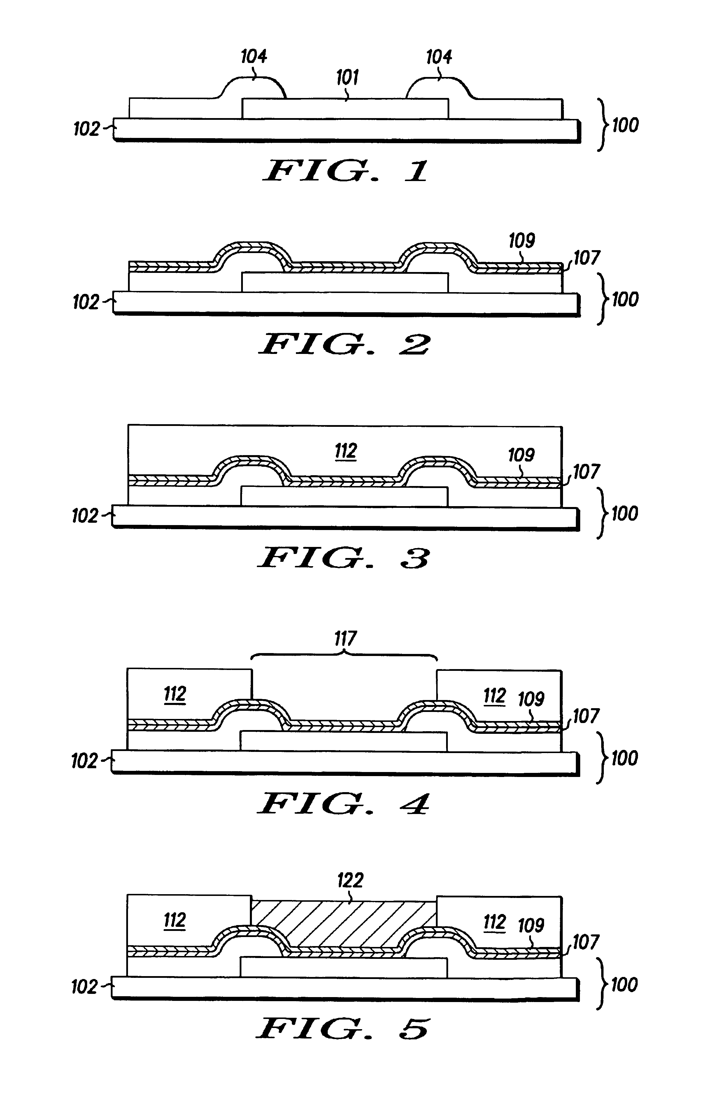
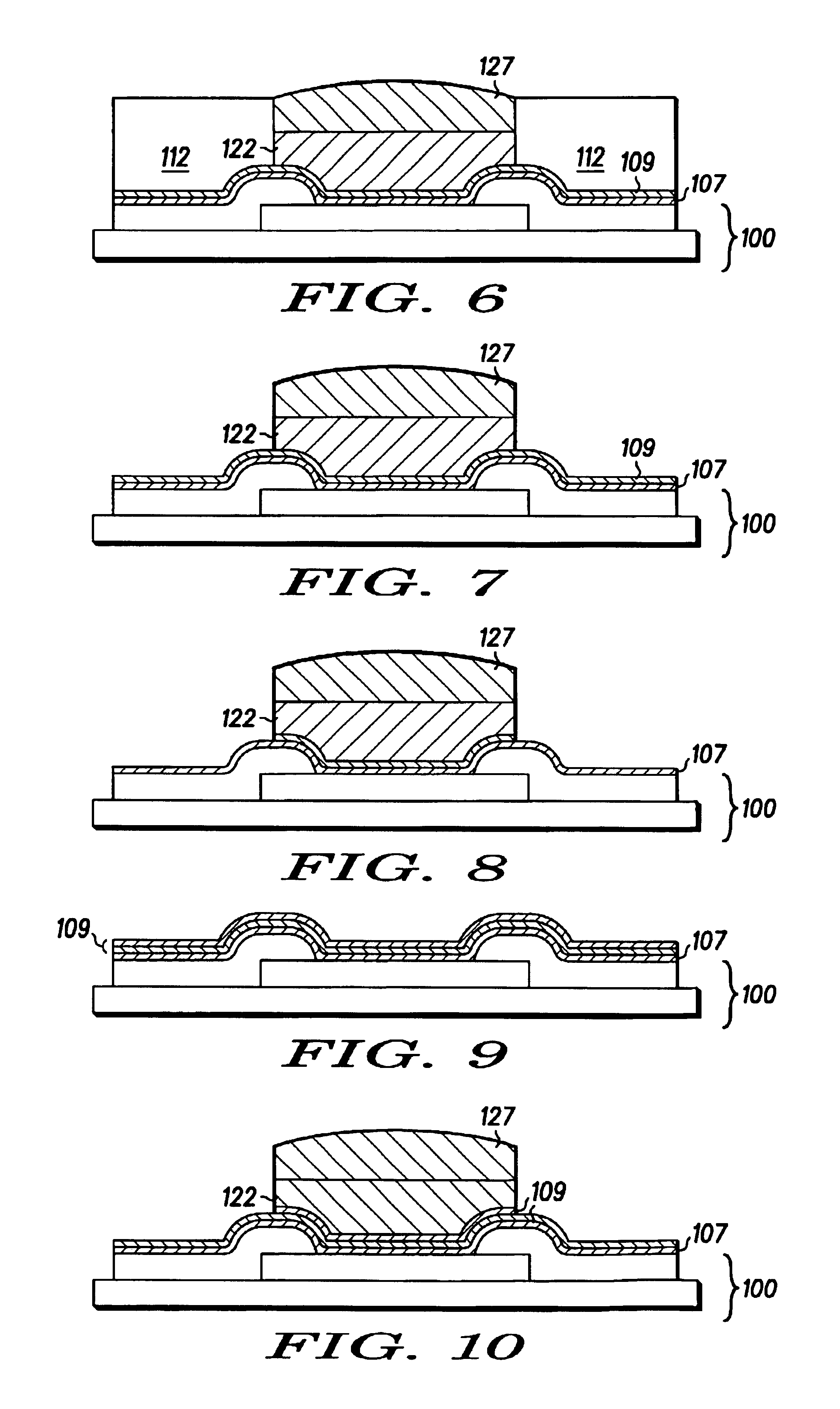
[0034]The following descriptions are of exemplary embodiments of the invention and the inventors' conceptions of the best mode and are not intended to limit the scope, applicability or configuration of the invention in any way. Rather, the following description is intended to provide convenient illustrations for implementing various embodiments of the invention. As will become apparent, changes may be made in the function and / or arrangement of any of the elements described in the disclosed exemplary embodiments without departing from the essence and scope of the invention.

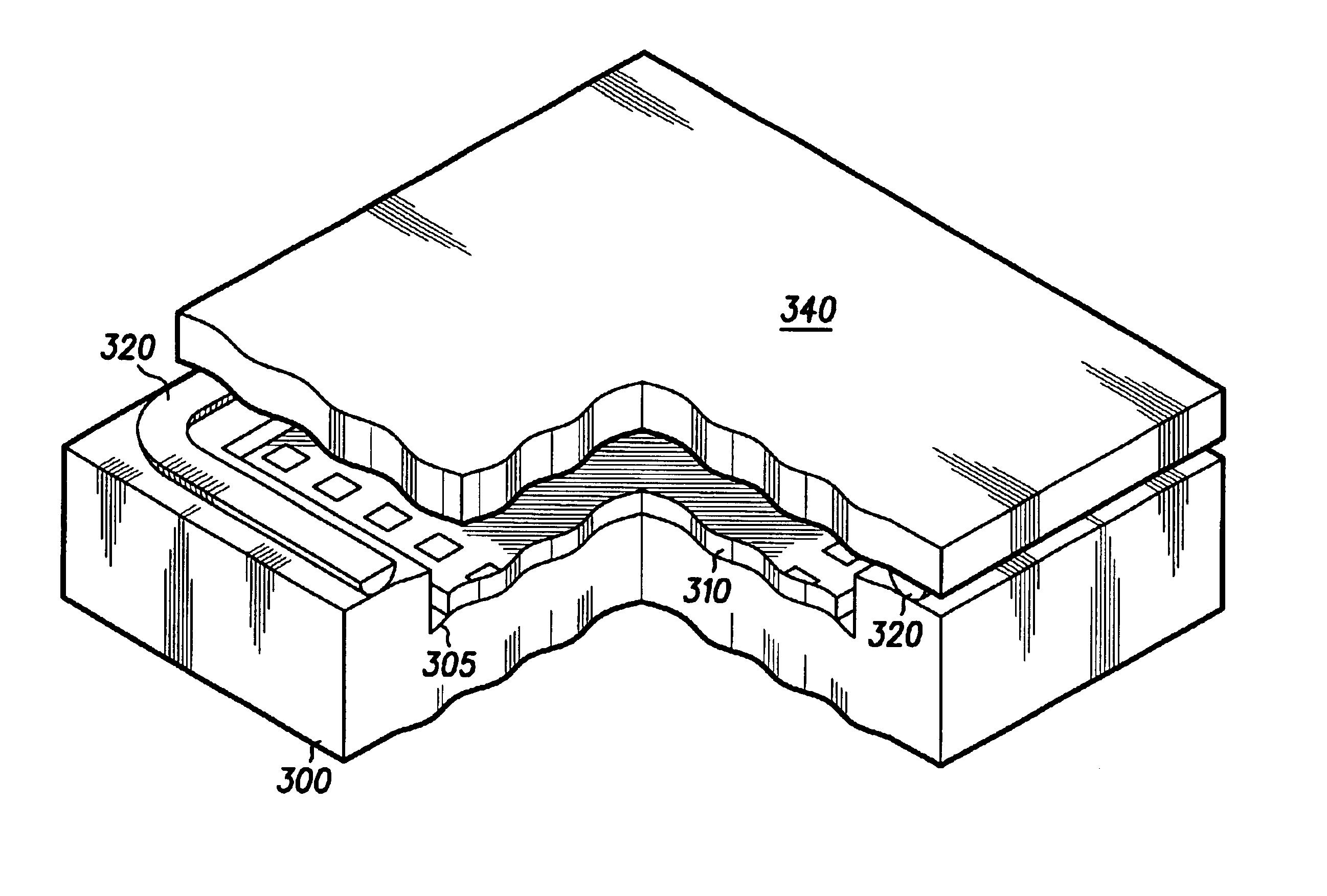
[0035]Various representative implementations of the present invention may be applied to any microelectromechanical system and / or method. Certain representative implementations may include, for example: RF shielding of discrete RF MEMS devices; RF shielding of arrays of RF MEMS device elements; wafer level hermetic packaging of MEMS devices; and wafer level testing and / or processing of sealed MEMS device arrays.

[003...


PUM


Abstract

An exemplary method and apparatus for MEMS device wafer level and / or array packaging comprises inter alia an EM shielding array of dielectric lid elements (340) sealed to a MEMS device die array (300) to produce a sealed MEMS device package array (330). Disclosed features and specifications may be variously controlled, adapted or otherwise optionally modified to improve hermetic sealing and / or EM shielding for any MEMS device. An exemplary embodiment of the present invention representatively provides for wafer level packaging of RF MEMS switches prior to device singulation.

Description

FIELD OF INVENTION[0001]The present invention generally relates to MEMS device fabrication and more particularly, in one representative and exemplary aspect, to wafer level packaging of RF MEMS devices prior to wafer dicing.BACKGROUND[0002]In general, microelectromechanical systems (MEMS) are miniature devices combining both electrical and mechanical components that are typically fabricated with batch-processing techniques borrowed from integrated circuit (IC) manufacturing technology. See, for example, J. Bryzek et al., “Micromachines on the March”, IEEE Spectrum Mag., May 20, 1994. Examples of representative MEMS devices include: accelerometers; optical switches; gyroscopes; sensors and actuators. Integrated MEMS (IMEMS) generally combine IC's with MEMS devices on a substantially unitary substrate. In either case, MEMS and IMEMS devices are usually adapted to employ spatially active elements (i.e., gears, pivots, hinges, levers, slides, etc.) which typically must be free to move i...

Claims


Application Information

Patent Timeline
IPC IPC(8): B81B7/00H01L21/50H01L21/02H01L23/552
CPCB81B7/0064H01L21/50H01L23/552H01L24/03H01L24/11H01L2224/0401H01L2224/1147H01L2224/11901H01L2224/13023H01L2224/13099H01L2924/01005H01L2924/01006H01L2924/01013H01L2924/01014H01L2924/01015H01L2924/01022H01L2924/01027H01L2924/01028H01L2924/01029H01L2924/0104H01L2924/01042H01L2924/01046H01L2924/01047H01L2924/0105H01L2924/01073H01L2924/01074H01L2924/01075H01L2924/01078H01L2924/01079H01L2924/01082H01L2924/01322H01L2924/014H01L2924/05042H01L2924/09701H01L2924/10329H01L2924/14H01L2924/1423H01L2924/19041H01L2924/30107H01L2924/3011H01L2924/3025H01L2924/01019H01L2924/01023H01L2924/01024H01L2924/01033H01L2924/01041H01L2924/01072H01L2924/10253H01L2924/00H01L2924/351H01L2924/15787H01L2924/181H01L2924/12042
Inventor LIN, JONG-KAILYTLE, WILLIAM H.FAY, OWENMARKGRAF, STEVENHUGHES, HENRY G.AMRINE, CRAIGDE SILVA, ANANDA P.
Owner NORTH STAR INNOVATIONS
Why Eureka
Try Eureka