Transistors having buried p-type layers beneath the source region

a technology of transistors and source regions, applied in the field of transistors, can solve the problems of limited power handling capability of such devices at higher operating frequencies, large heat generation of high-power and high-frequency transistors, and limited power handling capability of previously known jfets

Inactive Publication Date: 2005-10-18
CREE INC
View PDF58 Cites 38 Cited by
  • Summary
  • Abstract
  • Description
  • Claims
  • Application Information

AI Technical Summary

Problems solved by technology

Previously, bipolar transistors and power metal-oxide semiconductor field effect transistors (MOSFETs) have been used for high power applications but the power handling capability of such devices may be limited at higher operating frequencies.
Junction field-effect transistors (JFETs) were commonly used for high frequency applications but the power handling capability of previously known JFETs may also be limited.
In turn, high power and high frequency transistors usually generate larger amounts of heat than small signal transistors.
Although these devices provided increased operating frequencies and moderately increased power handling capability, the relatively low breakdown voltage and the lower thermal conductivity of these materials have limited their usefulness in high power applications.
Unfortunately, difficulty in manufacturing has limited the usefulness of SiC for high power and high frequency applications.
Although the SiC on Si substrate devices described in U.S. Pat. Nos. 4,762,806 and 4,757,028 may have exhibited improved thermal characteristics, the use of a Si substrate generally limits the ability of such devices to dissipate heat.
Furthermore, the growth of SiC on Si generally results in defects in the epitaxial layers that result in high leakage current when the device is in operation.
These devices typically provide adequate breakdown voltages as well as low leakage currents, but may sacrifice device performance due to unwanted trapping effects in the substrate.
However, these devices generally contain excessive parasitics that may degrade the RF performance of the device.

Method used


Image

  • Transistors having buried p-type layers beneath the source region
  • Transistors having buried p-type layers beneath the source region
  • Transistors having buried p-type layers beneath the source region

Examples


Embodiment Construction

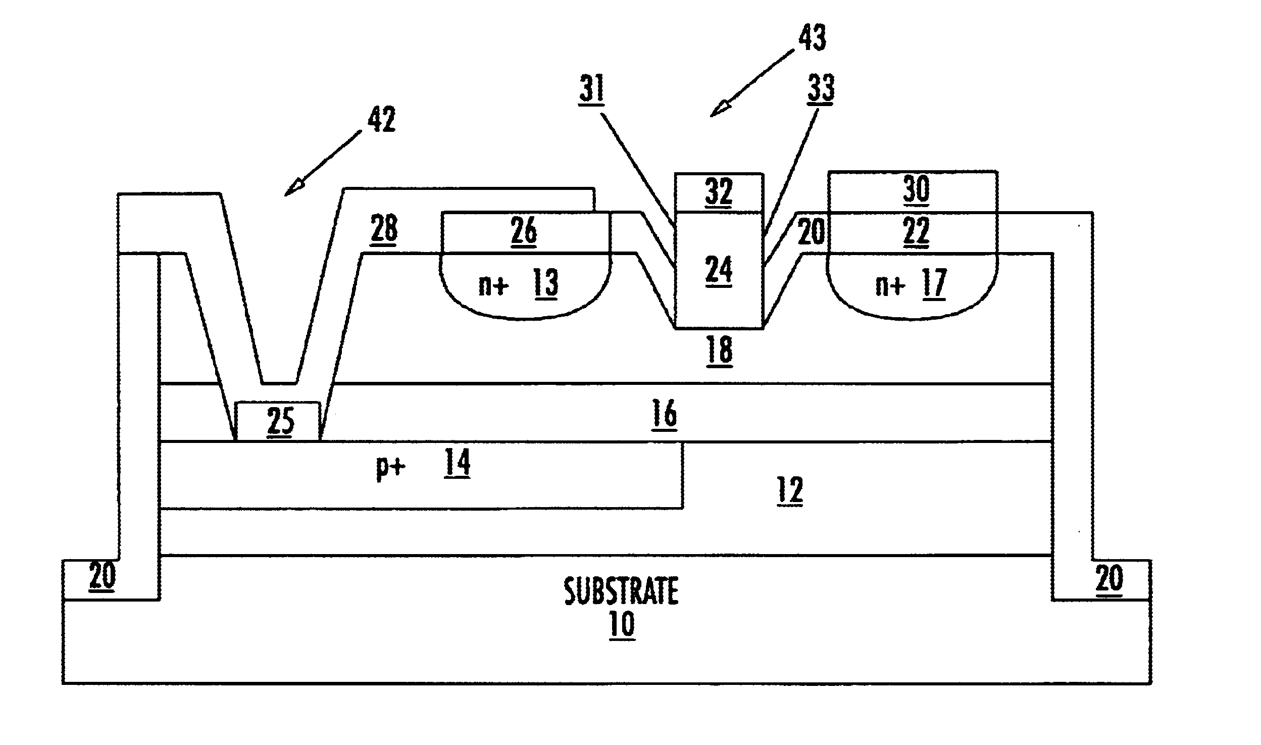
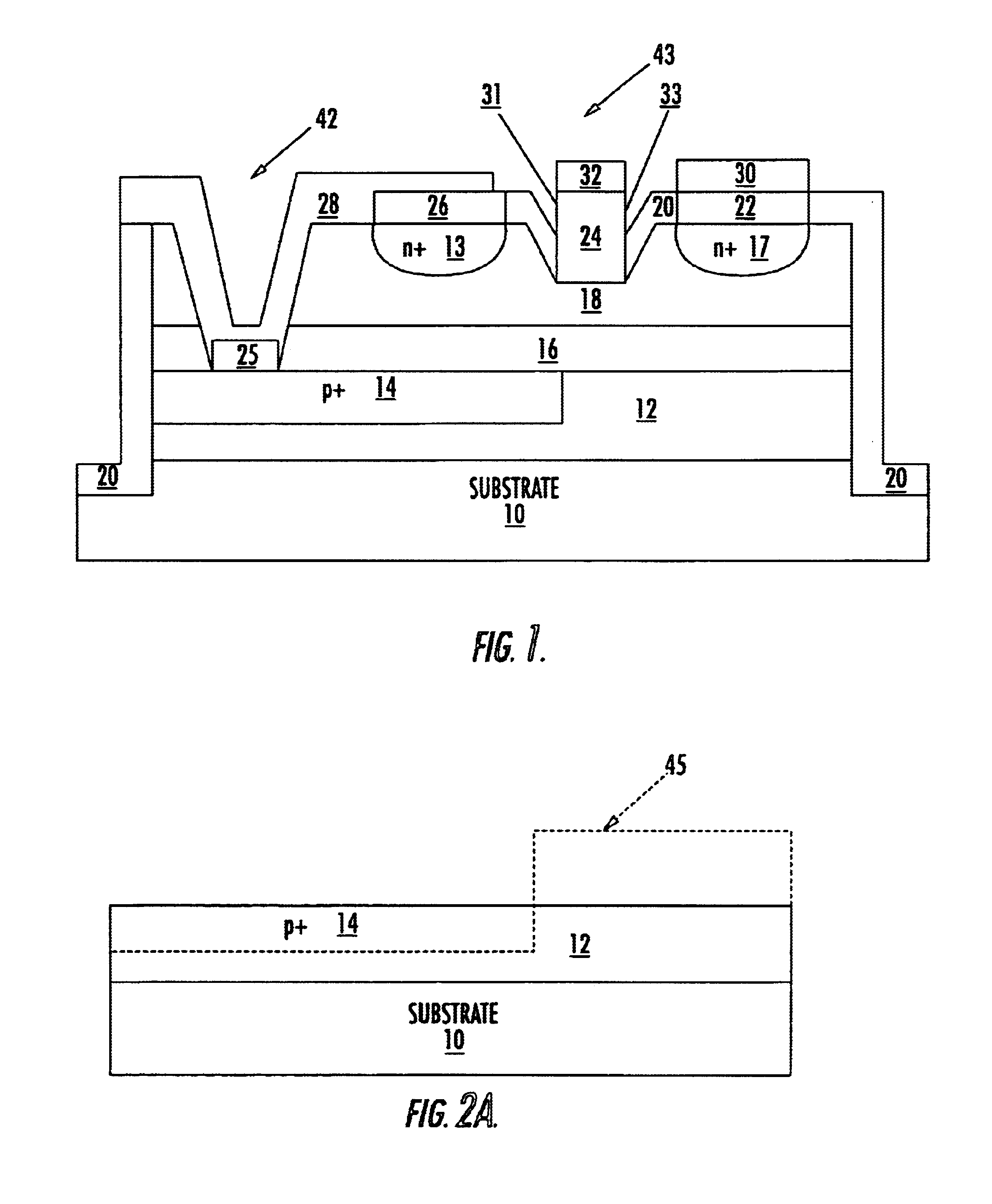
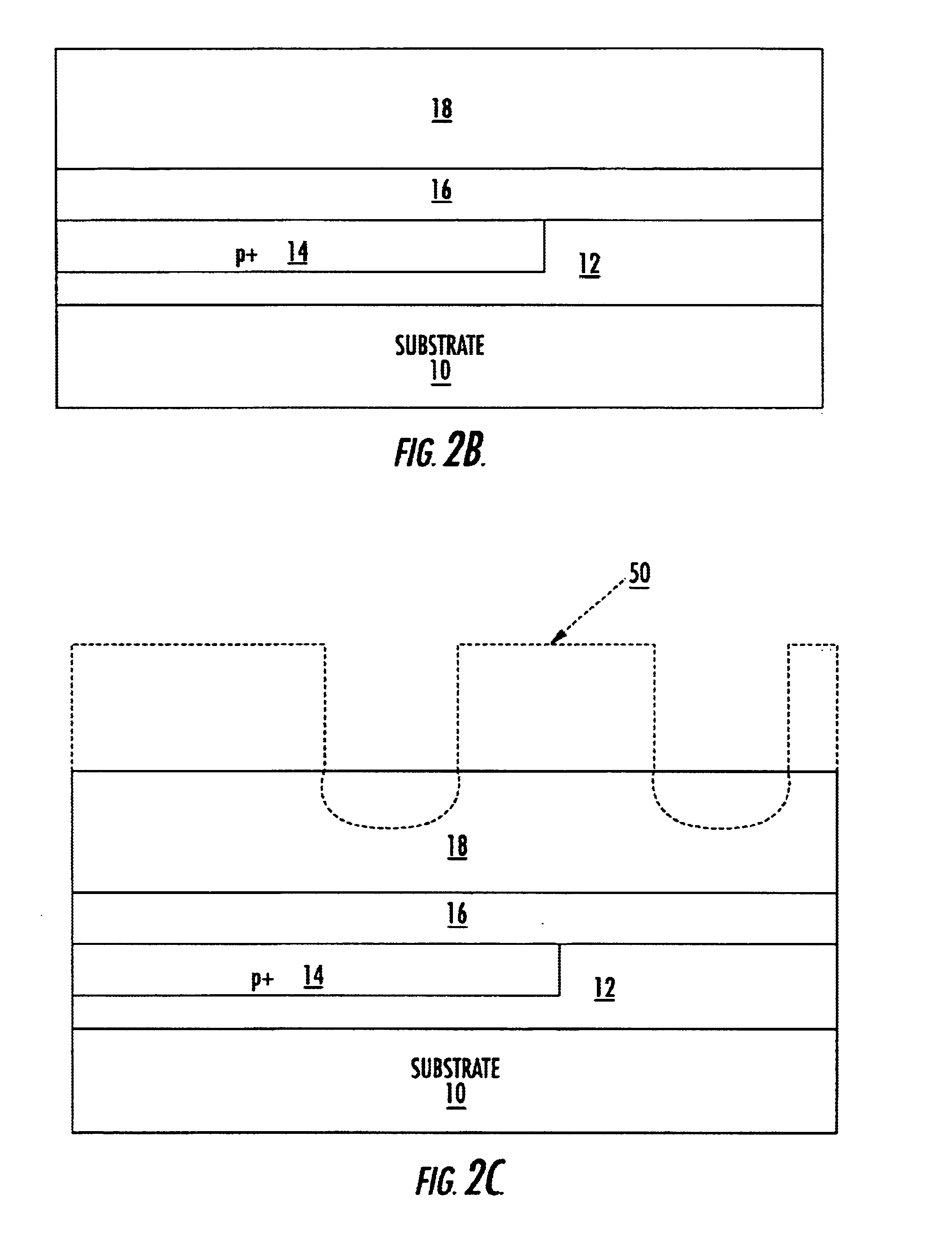
[0041]The present invention will now be described with reference to the FIGS. 1 through 8B, which illustrate various embodiments of the present invention. As illustrated in the Figures, the sizes of layers or regions are exaggerated for illustrative purposes and, thus, are provided to illustrate the general structures of the present invention. Furthermore, various aspects of the present invention are described with reference to a layer being formed on a substrate or other layer. As will be appreciated by those of skill in the art, references to a layer being formed “on” another layer or substrate contemplates that additional layers may intervene. References to a layer being formed on another layer or substrate without an intervening layer are described herein as being formed “directly on” the layer or substrate. Furthermore, relative terms such as beneath may be used herein to describe one layer or regions relationship to another layer or region as illustrated in the Figures. It wil...


PUM


Abstract

The present invention provides a unit cell of a metal-semiconductor field-effect transistor (MESFET). The unit cell of the MESFET includes a source, a drain and a gate. The gate is disposed between the source and the drain and on an n-type conductivity channel layer. A p-type conductivity region is provided beneath the source and has an end that extends towards the drain. The p-type conductivity region is spaced apart from the n-type conductivity channel region and is electrically coupled to the source.

Description

STATEMENT OF GOVERNMENT INTEREST[0001]This invention was made with Government support under N39997-99-C-3761 and N00014-96-C-2152 awarded by the Department of the Navy. The Government has certain rights in this invention.FIELD OF THE INVENTION[0002]The present invention relates to microelectronic devices and more particularly to transistors, for example, metal-semiconductor field-effect transistors (MESFETs).BACKGROUND OF THE INVENTION[0003]Electrical circuits requiring high power handling capability (>20 watts) while operating at high frequencies such as radio frequencies (500 MHz), S-band (3 GHz) and X-band (10 GHz) have in recent years become more prevalent. Because of the increase in high power, high frequency circuits there has been a corresponding increase in demand for transistors that are capable of reliably operating at radio frequencies and above while still being capable of handling higher power loads. Previously, bipolar transistors and power metal-oxide semiconductor...

Claims


Application Information

Patent Timeline
Patent Type & Authority Patents(United States)
IPC IPC(8): H01L29/66H01L21/02H01L21/338H01L21/04H01L29/812H01L29/24H01L29/20H01L29/02
CPCH01L29/8128H01L29/66856H01L29/812H01L29/66068H01L29/1608H01L29/2003
Inventor SRIRAM, SAPTHARISHI
Owner CREE INC
Why Eureka
Try Eureka