Integrated circuit stacking system and method

a stacking system and integrated circuit technology, applied in the field of integrated circuit stacking system and method, can solve the problems of adding cost and complexity topologies, and achieve the effect of reducing the overall footprint occupied by the ics and improving thermal performan

Inactive Publication Date: 2005-10-18
TAMIRAS PER PTE LTD LLC
View PDF113 Cites 88 Cited by
  • Summary
  • Abstract
  • Description
  • Claims
  • Application Information

AI Technical Summary

Benefits of technology

[0017]A form standard provides a physical form that allows many of the varying package sizes found in the broad family of CSP packages to be used to advantage while employing a standard connective flex circuitry design. In preferred modules, the flex circuitry is partially wrapped about a form standard. The form standard can take many configurations and may be used where flex circuitry is used to connect ICs to one another in stacked modules having two or more constituent ICs. For example, in stacked modules that include four levels of CSPs, three form standards are employed in preferred embodiments, although fewer may be used. In a preferred embodiment, the form standard will be devised of heat transference material, a metal for example, such as copper would be preferred

Problems solved by technology

Such techniques provide alternatives, but req

Method used


Image

  • Integrated circuit stacking system and method
  • Integrated circuit stacking system and method
  • Integrated circuit stacking system and method

Examples


Embodiment Construction

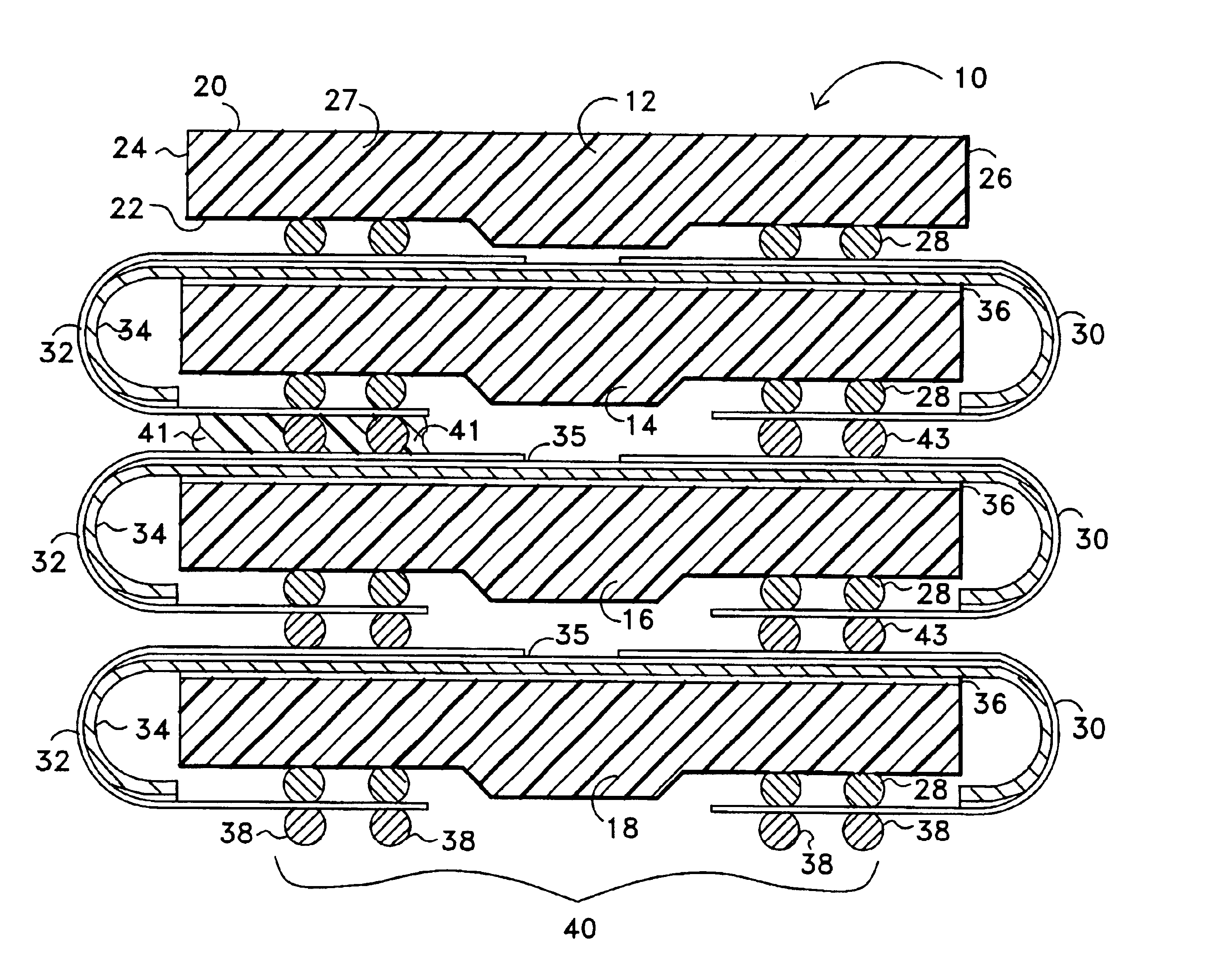
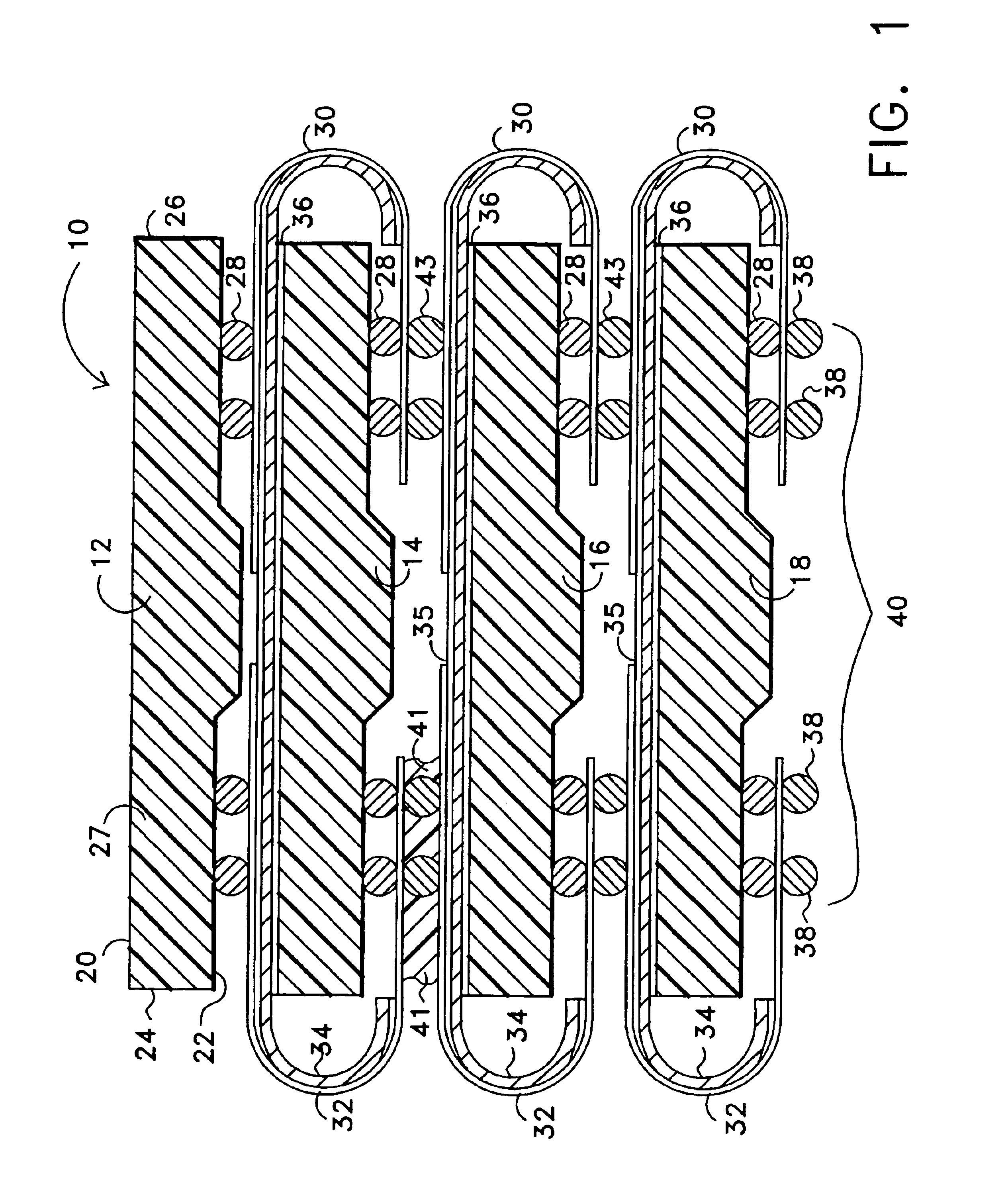
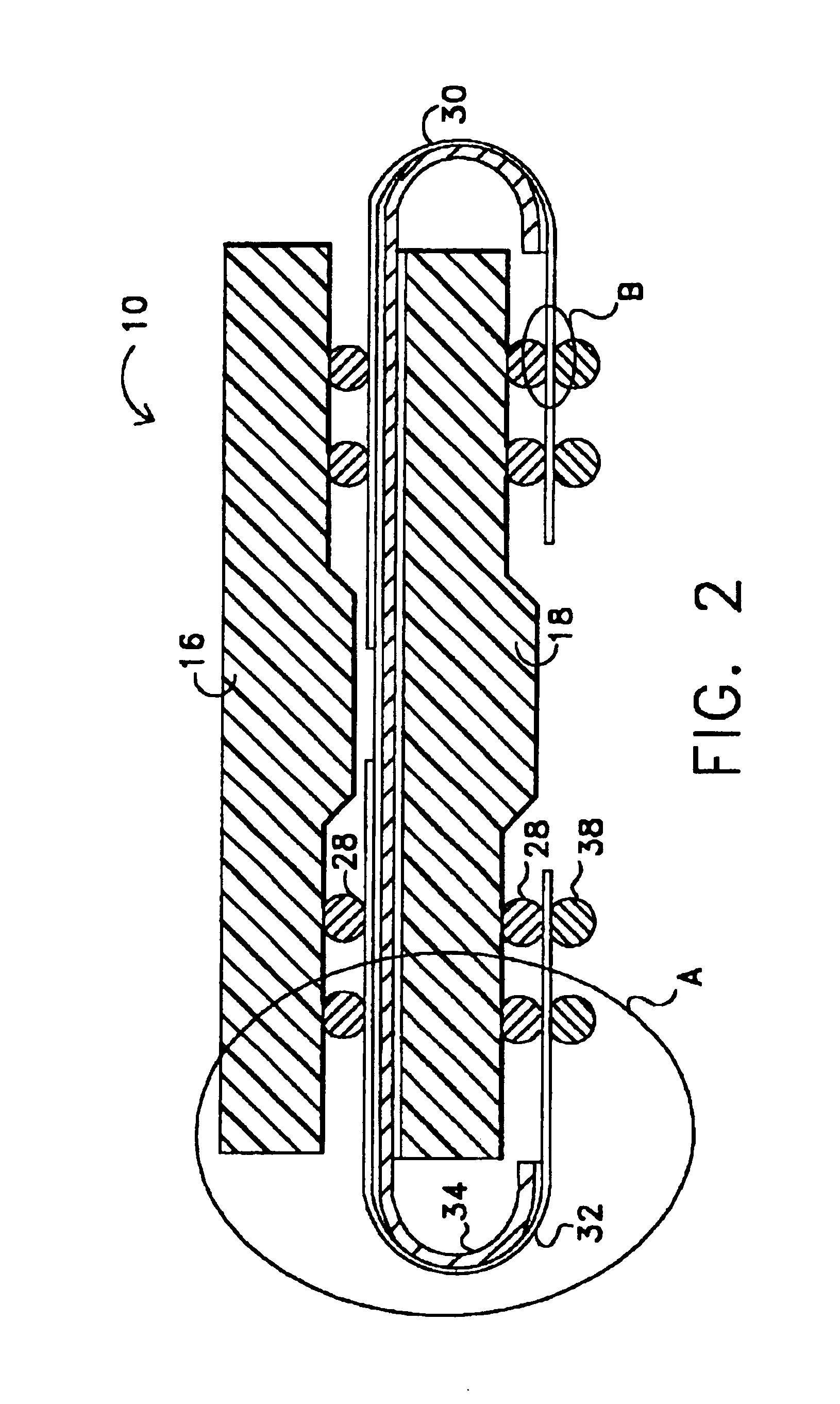
[0054]FIG. 1 is an elevation view of module 10 devised in accordance with a preferred embodiment of the present invention. Module 10 is comprised of four CSPs: level four CSP 12, level three CSP 14, level two CSP 16, and level one CSP 18. Each of the CSPs has an upper surface 20 and a lower surface 22 and opposite lateral edges 24 and 26 and typically include at least one integrated circuit surrounded by a plastic body 27. The body need not be plastic, but a large majority of packages in CSP technologies are plastic. Those of skill will realize that the present invention may be devised to create modules with different size CSPs and that the constituent CSPs may be of different types within the same module 10. For example, one of the constituent CSPs may be a typical CSP having lateral edges 24 and 26 that have an appreciable height to present a “side” while other constituent CSPs of the same module 10 may be devised in packages that have lateral edges 24 and 26 that are more in the ...


PUM


Abstract

The present invention stacks integrated circuits (ICs) into modules that conserve PWB or other board surface area. In another aspect, the invention provides a lower capacitance memory expansion addressing system and method and preferably with the CSP stacked modules provided herein. In a preferred embodiment in accordance with the invention, a form standard provides a physical form that allows many of the varying package sizes found in the broad family of CSP packages to be used to advantage while employing a standard connective flex circuitry design. In a preferred embodiment, the form standard will be devised of heat transference material such as copper to improve thermal performance. In an alternative embodiment, the form standard may include a heat spreader portion with mounting feet. In a preferred embodiment of the memory addressing system, a high speed switching system selects a data line associated with each level of a stacked module to reduce the loading effect upon data signals in memory access.

Description

RELATED APPLICATIONS[0001]This application is a continuation-in-part of PCT Pat. App. No. PCT / US03 / 29000, filed Sep. 15, 2003, pending, and of U.S. patent application Ser. No. 10 / 453,398, filed Jun. 3, 2003, pending, which is a continuation-in-part of U.S. patent application Ser. No. 10 / 005,581, filed Oct. 26, 2001, now U.S. Pat. No. 6,576,992. PCT Pat. App. No. PCT / US03 / 29000 and U.S. patent application Ser. No. 10 / 453,398 are incorporated by reference for all purposes.TECHNICAL FIELD[0002]The present invention relates to aggregating integrated circuits and, in particular, to stacking integrated circuits in chip-scale packages and providing such stacked integrated circuits on boards.BACKGROUND OF THE INVENTION[0003]A variety of techniques are used to stack packaged integrated circuits. Some methods require special packages, while other techniques stack conventional packages. In some stacks, the leads of the packaged integrated circuits are used to create a stack, while in other sys...

Claims


Application Information

Patent Timeline
IPC IPC(8): H01L23/48H01L23/538H01L23/52H01L23/31H01L23/28H01L23/498H01L25/10H05K1/14H05K3/36H05K1/18H01L23/02H01L23/367
CPCH01L23/3114H01L23/4985H01L23/5386H01L23/5387H01L25/105H05K1/141H05K1/147H01L2224/16237H01L2225/06517H01L2225/06541H01L2225/06579H01L2225/06586H01L2225/06589H01L2924/3011H05K1/189H05K3/363H05K2201/056H05K2201/10689H05K2201/10734H01L2924/01055H01L2225/107H01L2224/73204H01L2224/16225H01L2224/32225H01L2924/00012H01L2224/32145H01L2224/32245H01L2224/73253H01L2924/00014H01L2224/0401
Inventor CADY, JAMES W.WILDER, JAMESROPER, DAVID L.WEHRLY, JR., JAMES DOUGLAS
Owner TAMIRAS PER PTE LTD LLC
Why Eureka
Try Eureka