Multistage autozero sensing for a multilevel non-volatile memory integrated circuit system

a multi-level non-volatile memory and integrated circuit technology, applied in the field of semiconductor memories, can solve problems such as current ratio errors generated by mismatches

Inactive Publication Date: 2005-10-18
SILICON STORAGE TECHNOLOGY
View PDF9 Cites 72 Cited by
  • Summary
  • Abstract
  • Description
  • Claims
  • Application Information

AI Technical Summary

Problems solved by technology

The mismatch generates a current ratio error and may be caused by mismatches of the threshold voltage, the width, length, mobility, and oxide thickness of the circuit elements, such as transistors, in the signal paths.
The mismatch also may be caused by mismatch in signal paths due to parasitics, such as width and length of interconnects.

Method used


Image

  • Multistage autozero sensing for a multilevel non-volatile memory integrated circuit system
  • Multistage autozero sensing for a multilevel non-volatile memory integrated circuit system
  • Multistage autozero sensing for a multilevel non-volatile memory integrated circuit system

Examples


Embodiment Construction

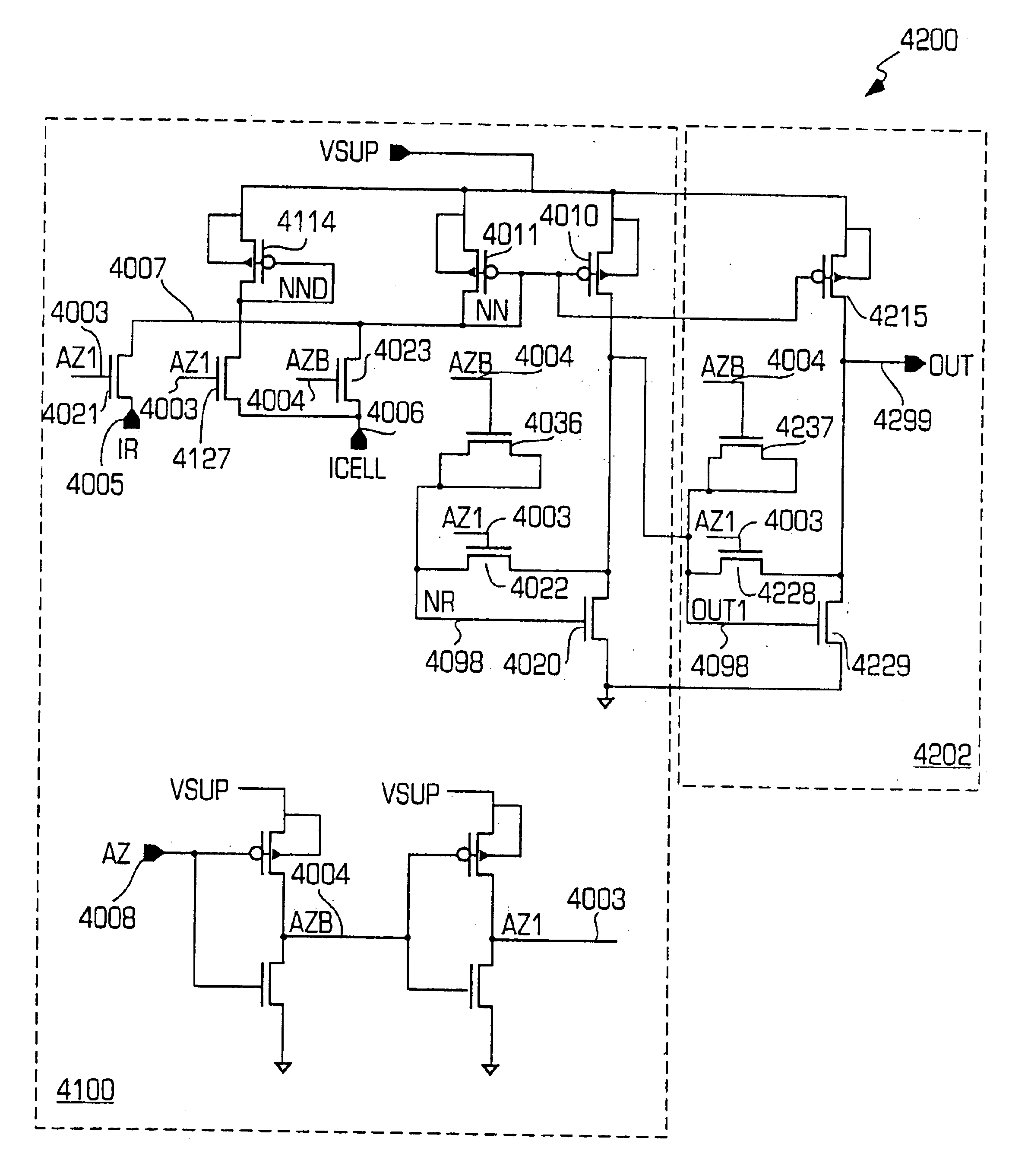
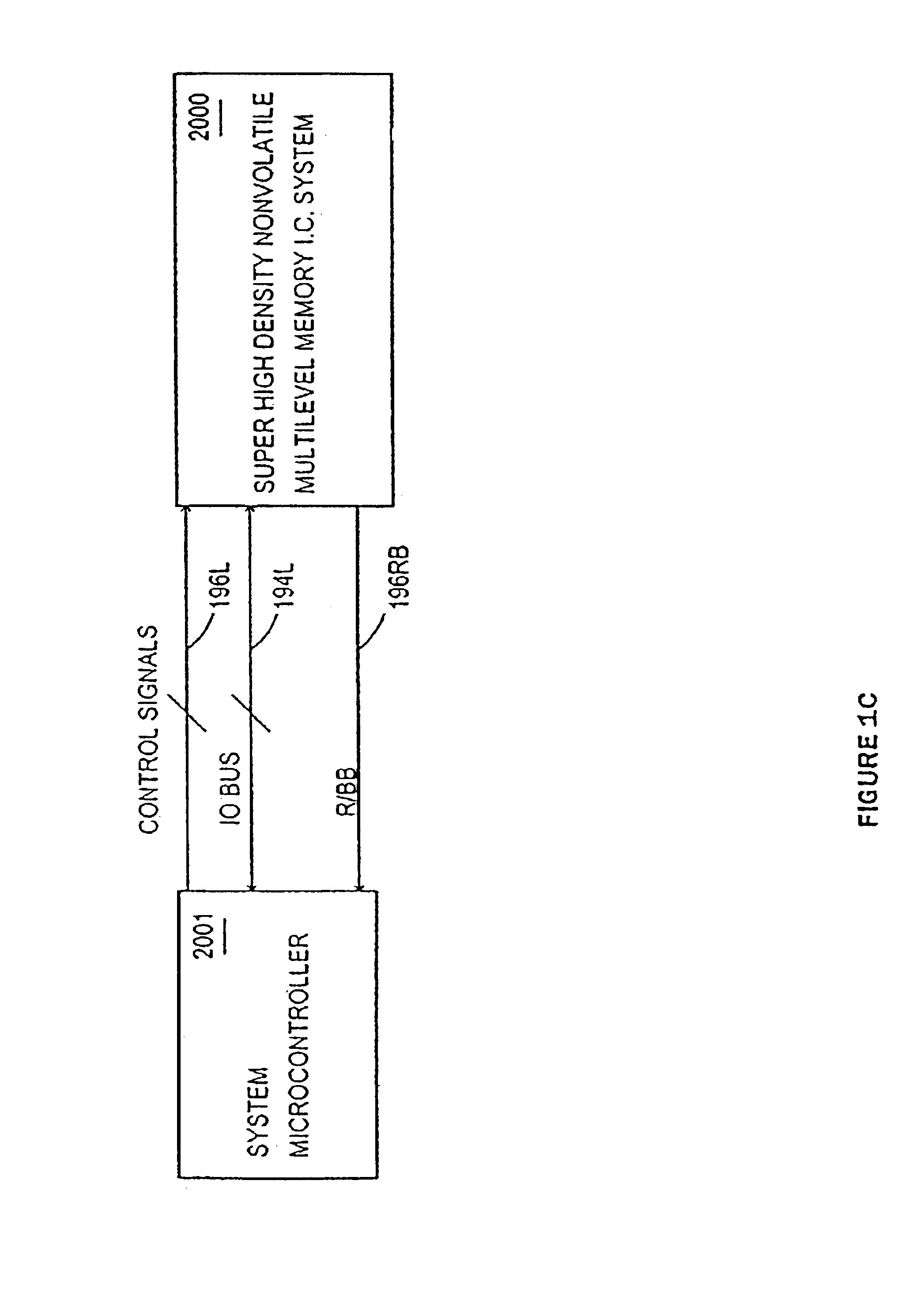
[0106]Described are the design method and apparatus for a super high density nonvolatile memory system capable of giga to tera bits as applied to the array architecture, reference system, and decoding schemes to realize the optimum possible number of storage levels within specified performance constraints. Method and apparatus for multilevel program and sensing algorithm and system applied to flash memory is also described.

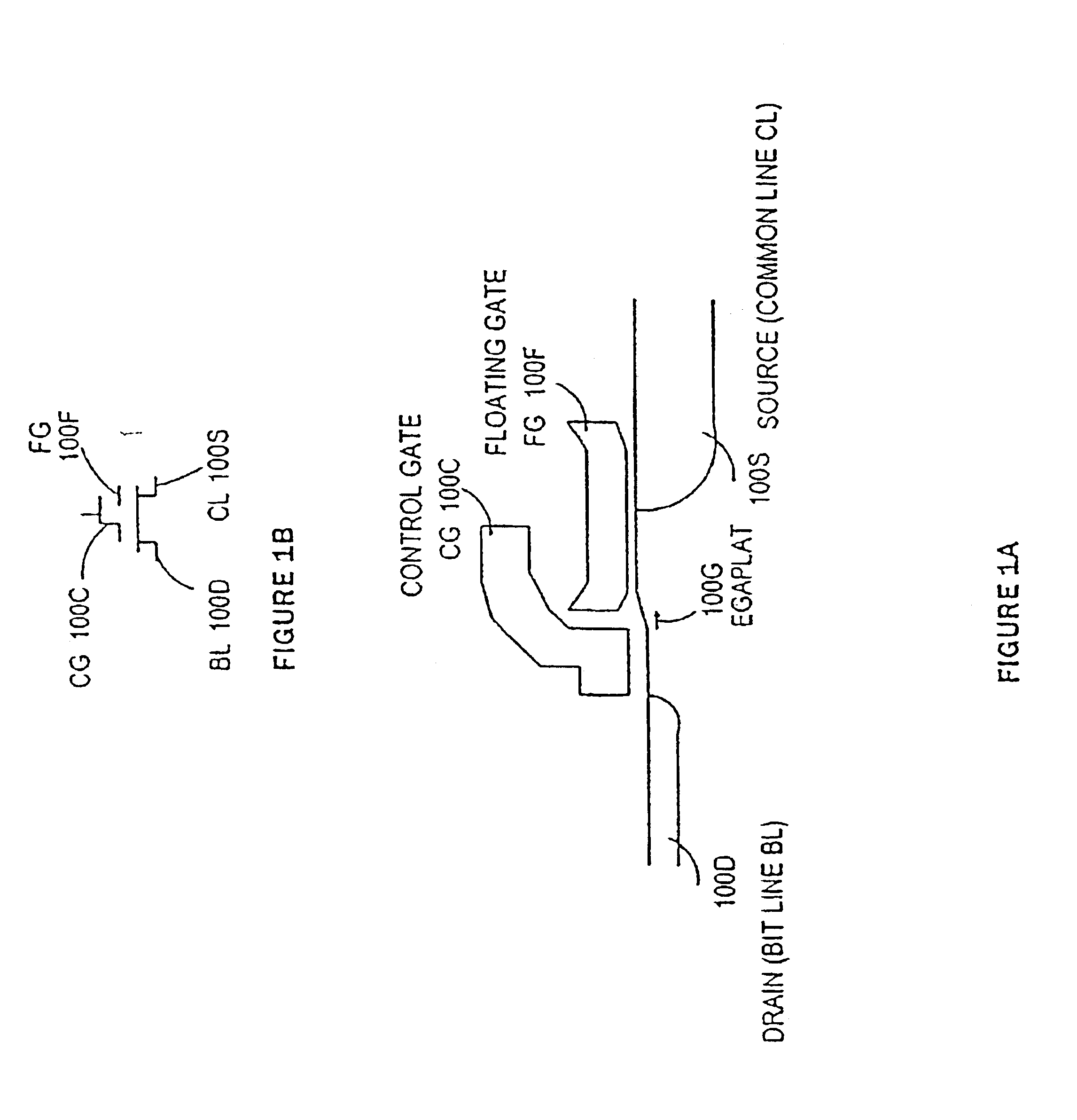
[0107]Array architectures and operating methods are described that are suitable for a super high density, in the giga to tera bits, for multilevel nonvolatile “green” memory integrated circuit system. “Green” refers to a system working in an efficient and low power consumption manner. The system and method solves the issues associated with super high density multilevel memory system, such as, precision voltage control in the array, severe capacitive loading from MOS transistor gates and parasitics, high leakage current due to memory cells and from cells to cells, ...


PUM


Abstract

A digital multibit non-volatile memory integrated system includes autozero multistage sensing. One stage may provide local sensing with autozero. Another stage may provide global sensing with autozero. A twisted bitline may be used for array arrangement. Segment reference may be used for each segment. The system may read data cells using a current sensing one or two step binary search. The system may use inverse voltage mode or inverse current mode sensing. The system may use no current multilevel sensing. The system may use memory cell replica sensing. The system may use dynamic sensing. The system may use built-in byte redundancy. Sense amplifiers capable of sub-volt (<<1V) sensing are described.

Description

CROSS-REFERENCE TO RELATED APPLICATIONS[0001]This is a continuation-in-part of application Ser. No. 10 / 211,886, filed Aug. 1, 2002, which is a continuation-in-part of application Ser. No. 09 / 929,542, filed Aug. 13, 2001 now U.S. Pat. No. 6,751,118, which is a division of application Ser. No. 09 / 231,928 filed Jan. 14, 1999, issued as U.S. Pat. No. 6,282,145, the subject matter of each of these applications is incorporated herein by reference.[0002]This application is related to U.S. patent application Ser. No. 10 / 317,409, filed on even date herewith, entitled “Digital Multilevel Memory System Having Multistage Autozero Sensing”, inventor Hieu Van Tran, the disclosure of which is incorporated herein by reference, U.S. patent application Ser. No. 10 / 317,375, filed on even date herewith, entitled “Digital Multilevel Non-Volatile Memory System”, inventor Hieu Van Tran, the disclosure of which is incorporated herein by reference, and U.S. patent application Ser. No. 10 / 317,433, filed on e...

Claims


Application Information

Patent Timeline
Patent Type & Authority Patents(United States)
IPC IPC(8): G11C16/06G11C11/56G11C16/10G11C16/28G11C16/08G11C16/24G11C27/00
CPCG11C11/5621G11C11/5628G11C11/5635G11C11/5642G11C11/5678G11C16/08G11C16/10G11C16/24G11C16/28G11C27/005G11C13/0004G11C2211/5634
Inventor TRAN, HIEU VAN
Owner SILICON STORAGE TECHNOLOGY
Why Eureka
Try Eureka