Methods and systems for high-aspect-ratio gapfill using atomic-oxygen generation

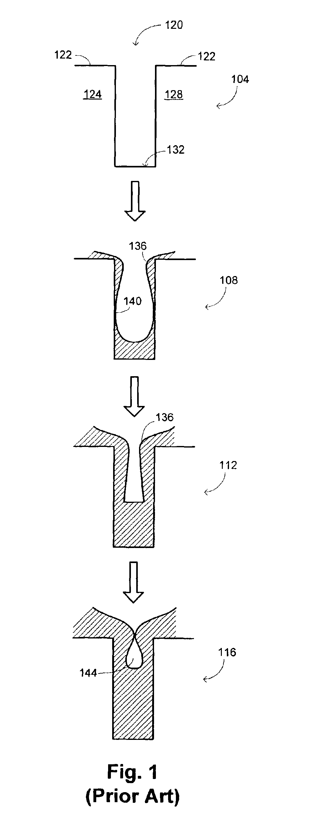
a technology of atomic oxygen and high-aspect ratio, applied in the direction of solid-state diffusion coating, vacuum evaporation coating, coating, etc., can solve the problems of increasing the aspect ratio, progressively more difficult to fill the gaps without leaving voids, and the width of these gaps decreases. , to achieve the effect of improving the redeposition characteristics

Inactive Publication Date: 2005-10-25
APPLIED MATERIALS INC
View PDF125 Cites 79 Cited by
  • Summary
  • Abstract
  • Description
  • Claims
  • Application Information

AI Technical Summary

Benefits of technology

[0008]Embodiments of the invention thus provide a method for depositing silicon within a gap on a substrate that produces improved redeposition characteristics. The inventors have identified that in addition to Ar, a further significant source of redeposition is the presence of molecular-oxygen ions in the plasma of a SiH4+O2 HDP-CVD process, even while they provide the source of oxidation as an oxidizing gas reactant. Accordingly, the effect of such molecular-oxygen ions is reduced in embodiments of the invention by maintaining certain ionic-species distributions in the plasma. In particular, the plasma is constrained by the process conditions to have a greater density of ions having a single oxygen atom than a density of ions having more than one oxygen atom.

Problems solved by technology

One of the persistent challenges faced in the development of semiconductor technology is the desire to increase the density of circuit elements and interconnections on substrates without introducing spurious interactions between them.
As circuit densities increase, however, the widths of these gaps decrease, increasing their aspect ratios and making it progressively more difficult to fill the gaps without leaving voids.
The formation of voids when the gap is not filled completely is undesirable because they may adversely affect operation of the completed device, such as by trapping impurities within the insulative material.
The high reactivity of the species in the plasma reduces the energy required for a chemical reaction to take place, and thus lowers the temperature required for such CVD processes when compared with conventional thermal CVD processes.
Semiconductor manufacturers have discovered, however, that there is a practical limit to the aspect ratio of gaps that HDP-CVD processes are able to fill.
It has been reported that when such a process is used to fill certain narrow-width high-aspect-ratio gaps, the sputtering caused by argon in the process gas may hamper the gapfill efforts.
This, in turn, may result in the formation of a void in the gap if the upper areas of regrowth join before the gap is completely filled.

Method used


Image

  • Methods and systems for high-aspect-ratio gapfill using atomic-oxygen generation
  • Methods and systems for high-aspect-ratio gapfill using atomic-oxygen generation
  • Methods and systems for high-aspect-ratio gapfill using atomic-oxygen generation

Examples


Embodiment Construction

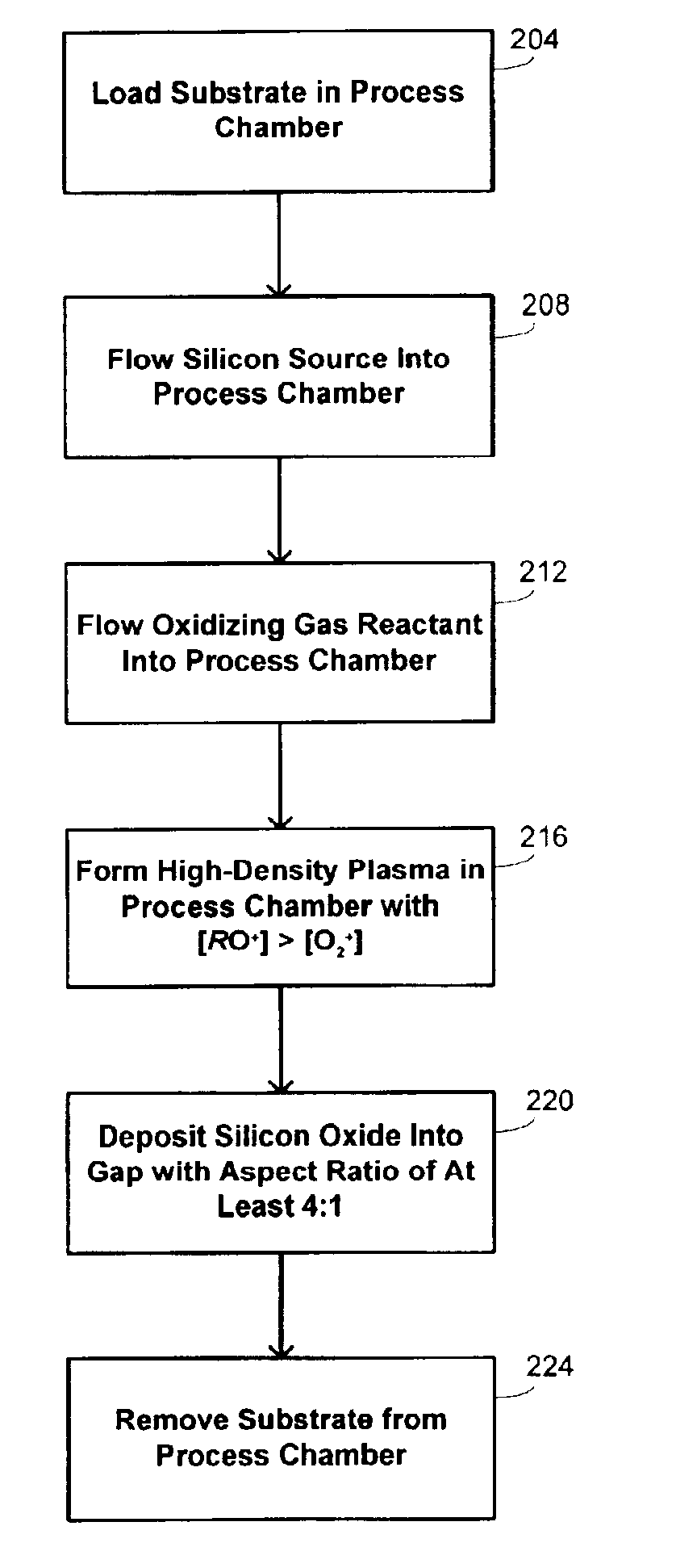
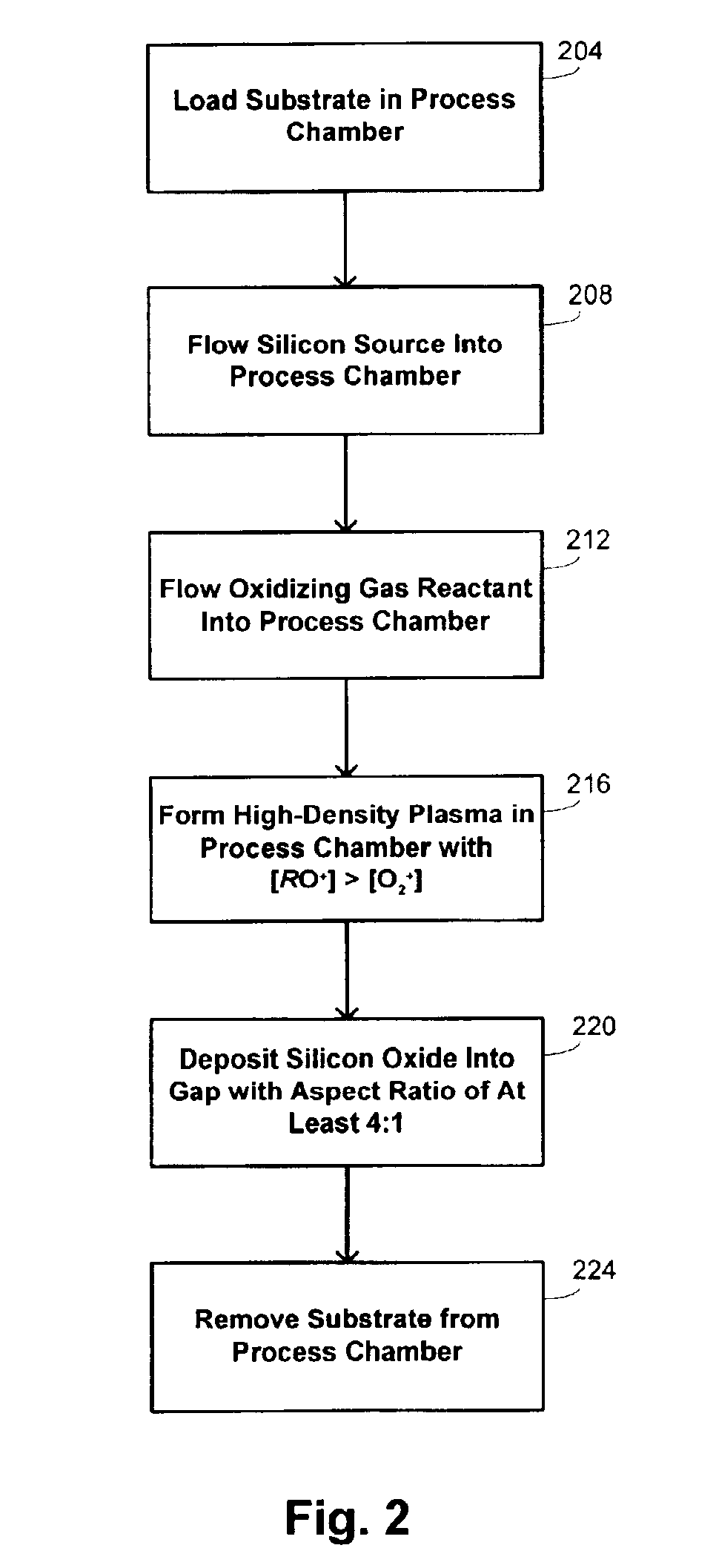
[0025]Embodiments of the invention are directed to a method of depositing a silicon oxide layer to fill a gap in a surface of a substrate using a high-density-plasma CVD process. Silicon oxide films deposited according to the techniques of the invention have excellent gapfill capabilities and are able to fill high-aspect-ratio gaps encountered in, for example, shallow-trench-isolation (“STI”) structures. Films deposited by the method of the invention are suitable for use in the fabrication of a variety of integrated circuits, and are particularly useful in the fabrication of integrated circuits having minimum feature sizes of 0.10 μm or less.

[0026]As used herein, a high-density-plasma process is a plasma CVD process that includes simultaneous deposition and sputtering components and that employs a plasma having an ion density on the order of 1011 ions / cm3 or greater. The relative levels of the combined deposition and sputtering characteristics of the high-density plasma may depend o...


PUM

PropertyMeasurementUnit
temperatureaaaaaaaaaa

Abstract

Methods and systems are provided for depositing silicon oxide in a gap on a substrate. The silicon oxide is formed by flowing a process gas into a process chamber and forming a plasma having an overall ion density of at least 1011 ions/cm3. The process gas includes H2, a silicon source, and an oxidizing gas reactant, and deposition into the gap is achieved using a process that has simultaneous deposition and sputtering components. The probability of forming a void is reduced by ensuring that the plasma has a greater density of ions having a single oxygen atom than a density of ions having more than one oxygen atom.

Description

BACKGROUND OF THE INVENTION[0001]One of the persistent challenges faced in the development of semiconductor technology is the desire to increase the density of circuit elements and interconnections on substrates without introducing spurious interactions between them. Unwanted interactions are typically prevented by providing gaps or trenches that are filled with electrically insulative material to isolate the elements both physically and electrically. As circuit densities increase, however, the widths of these gaps decrease, increasing their aspect ratios and making it progressively more difficult to fill the gaps without leaving voids. The formation of voids when the gap is not filled completely is undesirable because they may adversely affect operation of the completed device, such as by trapping impurities within the insulative material.[0002]Common techniques that are used in such gapfill applications are chemical-vapor deposition (“CVD”) techniques. Conventional thermal CVD pro...

Claims


Application Information

Patent Timeline
Patent Type & Authority Patents(United States)
IPC IPC(8): C23C16/04C23C16/507C23C16/40C23C16/50H01L21/70H01L21/762H01L21/02H01L21/316
CPCC23C16/045C23C16/402C23C16/507H01L21/02164H01L21/02274H01L21/31612H01L21/76227
Inventor KARIM, M. ZIAULMOGHADAM, FARHAD K.SALIMIAN, SIAMAK
Owner APPLIED MATERIALS INC
Why Eureka
Try Eureka