
Optimized contact design for flip-chip LED

a technology of flip-chip leds and contact design, applied in the field of optoelectronic devices, can solve problems such as not leading to an optimal solution, and achieve the effect of maximizing the contact area

Inactive Publication Date: 2005-10-25
EMCORE INC
View PDF19 Cites 108 Cited by
  • Summary
  • Abstract
  • Description
  • Claims
  • Application Information

AI Technical Summary

Benefits of technology

[0016]Preferably, the light-emitting diode further comprises a connection panel. The structure is mounted on the connection panel with the top surface facing toward the connection panel and the n-type region facing away from the connection panel. The connection panel preferably includes one or more p-connections and one or more n-connections. The p-pad preferably comprises one or more p-pads connected to the one or more p-connections. The n-pad preferably comprises one or more n-pads connected to the one or more n-connections. The p-connections may include solder balls that are disposed to maximize a contact area. The contact area acts as a heat sink. Preferably, the contact area covers at least 20% of the p-electrode.
[0017]In accordance with another aspect of the present invention, a light-emitting diode is provided. The light-emitting diode comprises a structure, a p-type electrode-pad unit, a trench and an n-type electrode pad unit. The structure includes a transparent substrate and regions of n-type and p-type GaN based semiconductor. The n-type GaN based semiconductor overlies the transparent substrate. The p-type GaN based semiconductor overlies the n-type region and defines a top surface remote from the transparent substrate. The structure defines an active light-emitting region between the n-type region and the p-type region. The structure has edges bounding the top surfa...

Problems solved by technology

However, even a nominally transparent electrode will absorb some of the light emitted in the die.
Although the U.S. Pat. No. 6,307,218 patent states that the same electrode designs used in a top-emitting die can be employed in a flip-chip die, this would not lead to an optimum solution.

Method used


Image

  • Optimized contact design for flip-chip LED
  • Optimized contact design for flip-chip LED
  • Optimized contact design for flip-chip LED

Examples


Embodiment Construction

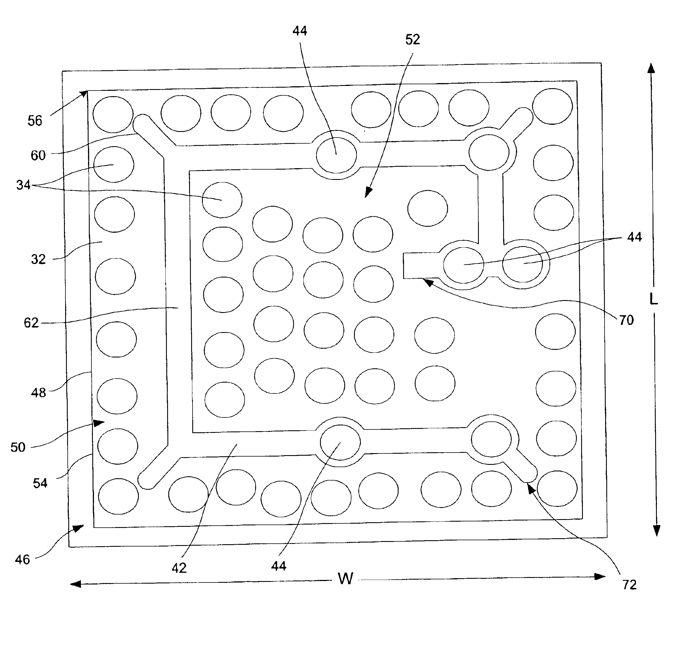
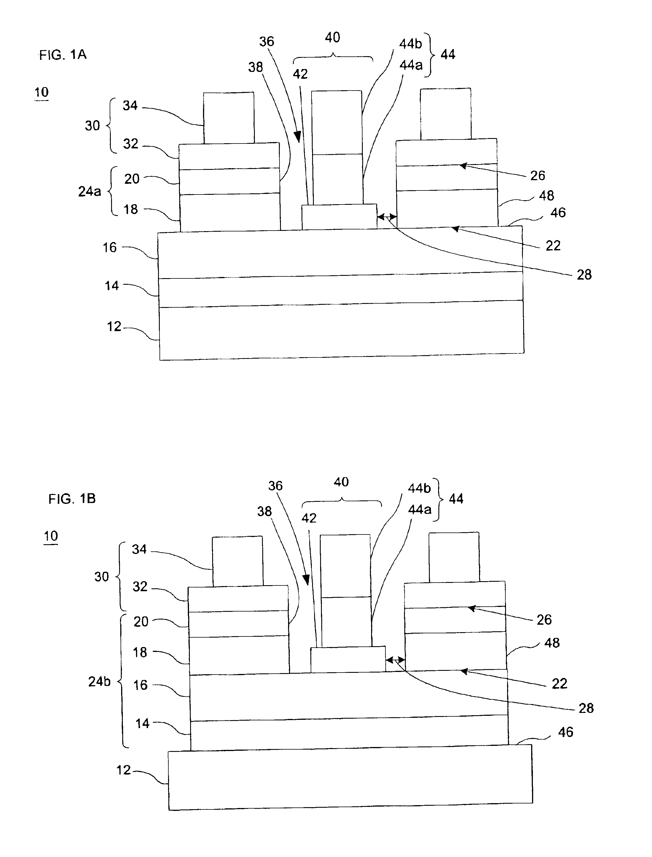
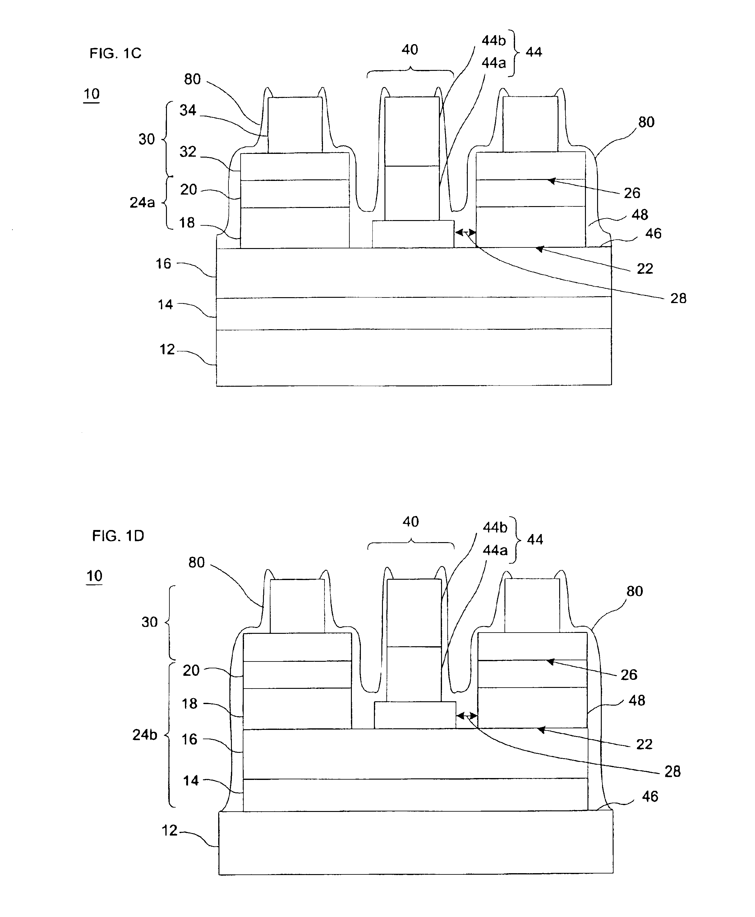
[0026]In accordance with one embodiment of the present invention, FIGS. 1A-F illustrate an LED 10 having a stacked structure of semiconductor layers on a substrate 12. The substrate 12 is preferably transparent. The substrate 12 may comprise gallium-nitride based materials, alumina, AlN, ZnO, silicon carbide (SiC), sapphire or other suitable materials. The structure and composition of the various layers incorporated in the stack and the sequence of layers in the stack may be selected according to known principles and techniques to provide the desired emission characteristics. The fabrication processes used to form the stacked structure are also well known. Most commonly, the various layers which form the stacked structure are deposited on the substrate 12 in sequence by techniques such as metal organic chemical vapor deposition (“MOCVD”), molecular beam epitaxy (“MBE”) and the like.

[0027]The stacked structure includes a first region 16 having a semiconductor material of a first type...


PUM


Abstract

Light emitting diodes are provided with electrode and pad structures that facilitate current spreading and heat sinking. A light emitting diode may be formed as a die with a stacked structure having a first region and a mesa projecting from a surface of the first region. A first electrode may substantially cover the mesa and have a plurality of pads disposed thereon maximizing a contact area in relation to the first electrode. A second electrode may be disposed as a trace on the surface of the first region, the trace having a spiral, segmented / interdigitated, loop or pattern. Optionally, the trace includes corner spikes projecting outwardly toward edges of the first electrode.

Description

BACKGROUND OF THE INVENTION[0001]The present invention relates to optoelectronic devices such as light-emitting diodes. In particular, the present invention relates to light-emitting diodes having an optimized contact geometry in a flip-chip configuration.[0002]Light-emitting diodes (“LEDs”) may include thin layers of semiconductor material of two opposite conductivity types, referred to as p-type and n-type. The layers may be disposed in a stack on a substrate. The stack may include one or more layers of n-type material in one part of the stack and one or more layers of p-type material in another part of the stack. The stacked material, including the substrate, may form a wafer. The wafer may be cut apart to form individual dies constituting separate LEDs. The junction between the p-type and n-type material (“the p-n junction”) may include directly abutting p-type and n-type layers, or may include one or more intermediate layers that may be of any conductivity type.[0003]In operati...

Claims


Application Information

Patent Timeline
IPC IPC(8): H01L33/00H01L33/20H01L33/38
CPCH01L33/38H01L33/20H01L2924/0002H01L2924/00
Inventor SHELTON, BRYANELIASHEVICH, IVANVENUGOPALAN, HARI
Owner EMCORE INC
Features
  • Generate Ideas
  • Intellectual Property
  • Life Sciences
  • Materials
  • Tech Scout
  • Unparalleled Data Quality
  • Higher Quality Content
  • 60% Fewer Hallucinations
Learn More