Three-transistor NAND and NOR gates for two-phase clock generators

a clock generator and logic gate technology, applied in logic circuits, pulse manipulation, pulse techniques, etc., can solve the problems of introducing perturbations and significant degrading of clock period stability, and achieve the effect of improving the jitter performance of the clock generator and simplifying the logic gate nand/nor

Active Publication Date: 2005-10-25
TEXAS INSTR INC
View PDF1 Cites 6 Cited by
  • Summary
  • Abstract
  • Description
  • Claims
  • Application Information

AI Technical Summary

Benefits of technology

[0004]The present invention achieves technical advantages by allowing the circuit designer to simplify the NAND / NOR logic gates used in non-overlapped phase generation circuits, eliminating 1 transistor out of 4 that can be proven redundant in a synchronization application. The associated reduction in the capacitive self-loading seen at the gate output advantageously enables much steeper fronts on the output voltage, eventually ameliorating the jitter performance of the whole clock generator.
[0005]The present invention may be incorporated in a novel clock structure implemented for a high speed (80 MSps) high-input frequency (for use in receivers with up to 225 MHz IF) 14-bit analog-to-digital converter (ADC), lowering the jitter from 530 fs down to 230 fs. To date, this ranks as the lowest jitter CMOS-based clock ever implemented and tested in an ADC. In turn, the jitter performance boosts the SNR performance of an ADC from about 60 dBFS at 80 MSps, 220 MHz input to as high as 67 dFS in the same conditions.
[0006]The present invention advantageously exploits the timing sequence of the signals driving a NAND gate. The present invention recognizes that since the pull-up operation of a node B2 is dictated by a node B1 only, keeping two PMOSFET devices in the NAND gate is redundant. In fact, the PMOSFET 46 driven by node A4 in FIG. 3, which will be described in detail shortly, covers an input-to-output transition which is possible in principle, but that never happens in practice when the NAND is embedded in the classical two-phase clock loop of FIG. 1. According to the present invention, the structure of the NAND gate 44 is simplified whereby the NAND gate essentially becomes an inverter driven by node B1, whose pulldown operation is only conditioned to node A4. In other words, the essence of the NAND logic is preserved through the series of two NMOSFETs, whereas the active pull-up can be guaranteed by utilizing only one PMOSFET.
[0007]The NAND gate of the present invention improves the clock generation and distribution on-chip, reducing the jitter of internal clock networks, and simplifies the structure of the NAND CMOS gates built inside the two-phase generator, providing an enhanced solution right at the very root of the problem. The principles and advantages of the present invention is also applicable to a NOR gate.

Problems solved by technology

The thermal noise of the logic gates, and especially the voltage bounce of the supply rails, can significantly degrade the stability of the clock period, introducing perturbations on the time of occurrence of the sampling edge which are inversely proportional to the slope of the waveforms featured at every node.

Method used


Image

  • Three-transistor NAND and NOR gates for two-phase clock generators
  • Three-transistor NAND and NOR gates for two-phase clock generators
  • Three-transistor NAND and NOR gates for two-phase clock generators

Examples


Embodiment Construction

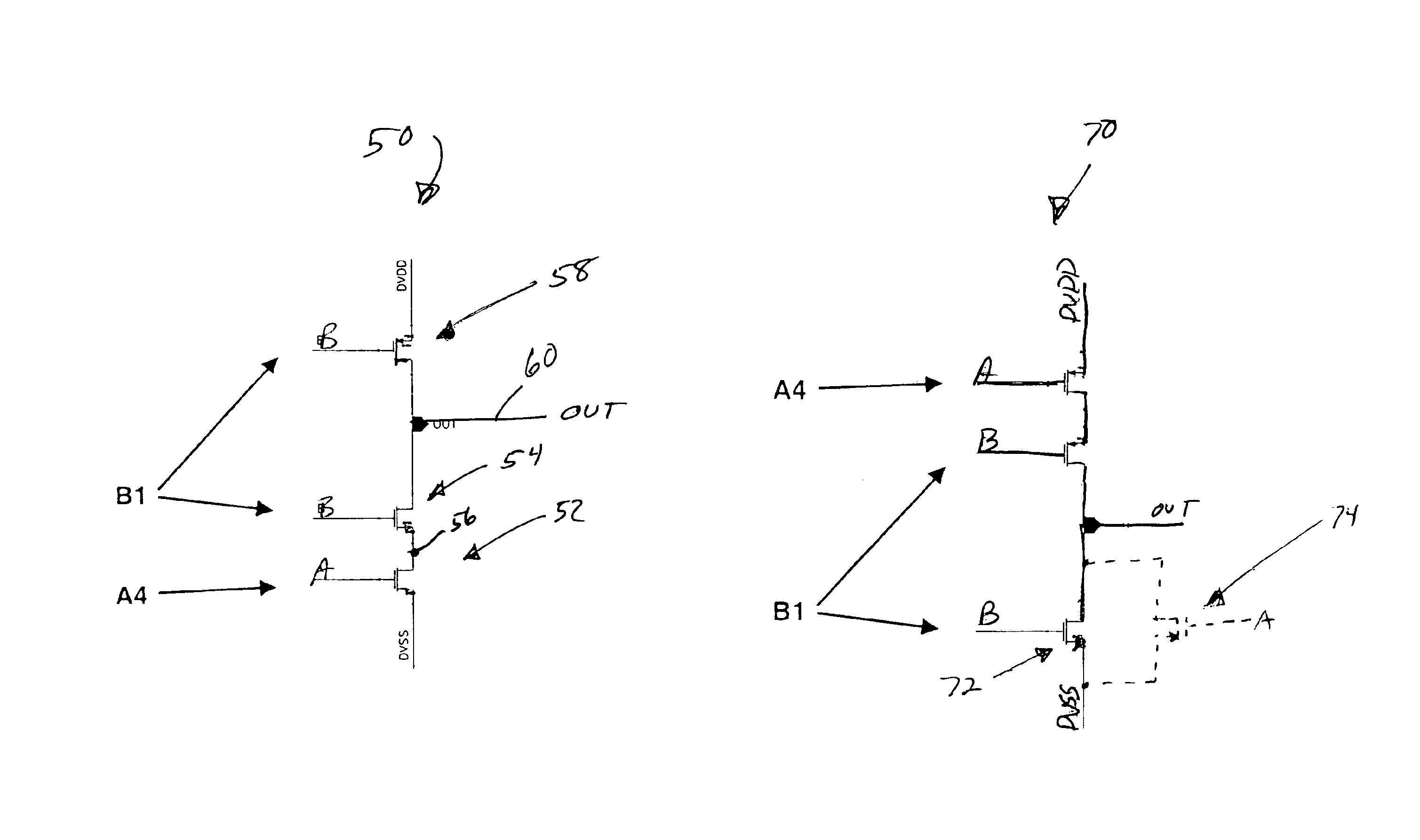
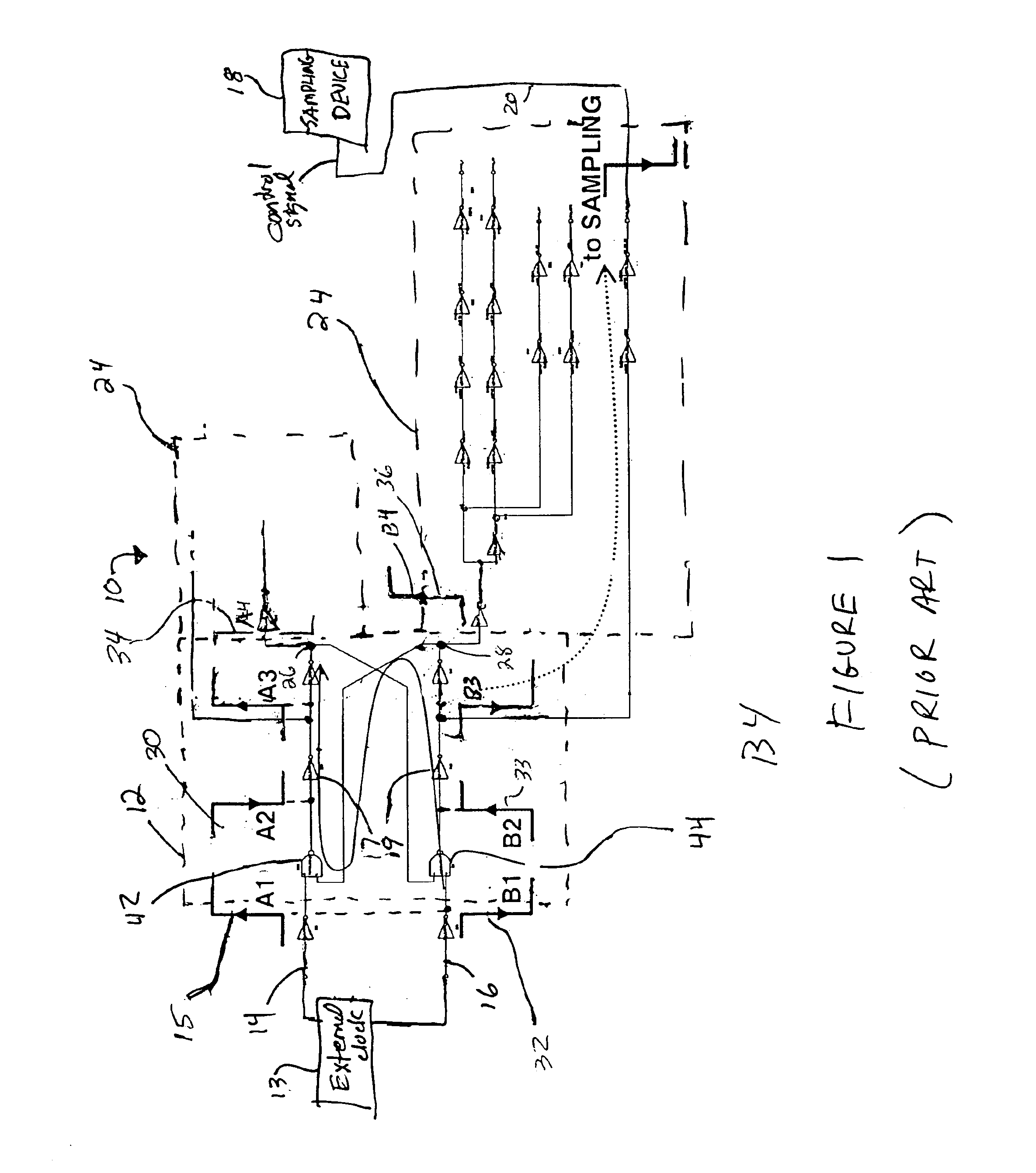
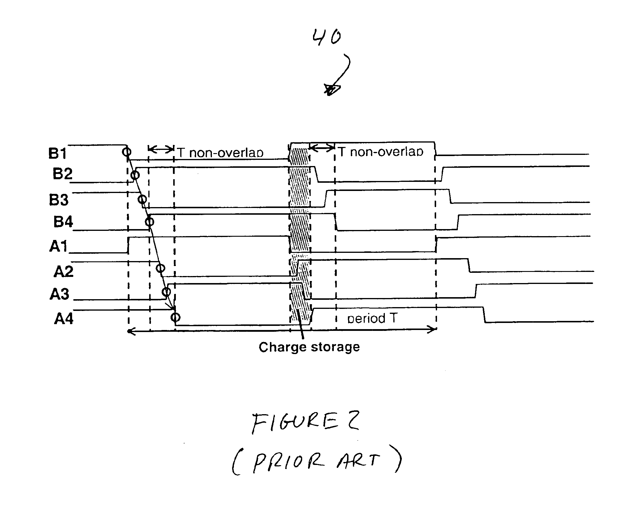
[0018]Referring to FIG. 1, there is shown a prior art clock generator circuit 10, having a 2 input 6-gate loop network shown at 12 which performs non-overlapping of the two phases provided at inputs 14 and 16, and outputs a synchronization signal to a sampling device 18 at output 20. An inverter tree 24 receives the respective output 26 and 28 of the loop 12 and is a tapered clock distribution / edge regeneration circuitry. If the sampling device 18 receiving output 20 is modeled as a simple NMOSFET switch connected to a sampling capacitor for ease of discussion, the timing sequence in circuit 12 shown at 32, 33, and 28 drives the HIGH→LOW edge that shuts down the sampling transistor 18 and constitutes the sampling event for the incoming signal.

[0019]The operating principle of the loop network circuit 12 is based on inducing a transition 34 at the output node A4 (26) of the non-overlapping network 12, which transition 34 is not aligned with the complementary transition 36 at output no...


PUM


Abstract

A two-phase non-overlapping clock generator (12) generating a sampling signal (20) utilizing a three transistor NAND gate (50). The NAND gate of the present invention eliminates one large PMOSFET (46), and has one NMOSFET (52) driven by the other phase and having its source grounded. The present invention yields substantial improvement on the jitter of the clock phases. Both rising and falling transitions are improved because of the greatly reduced self-loading of the NAND gate. Overshooting is eliminated, and the NAND gate body effect is minimized, providing enhanced jitter performance of the sampling signal and improving a signal to noise ratio (SNR). The principle of the present invention are also embodied in a NOR gate (70).

Description

FIELD OF THE INVENTION[0001]The present invention is generally related to precision signal sampling circuits, and more particularly to sampling signals sensitive to signal-to-noise ratios, such as two-phase clock generators used in analog circuits including high-speed analog-to-digital converters (ADC's).BACKGROUND OF THE INVENTION[0002]In high-speed ADC applications, as well as in every other instance when sampling of an analog signal is involved (i.e. optical receivers, data stream “slicers”, etc.), the precision of the sampling instant impacts the signal-to-noise ratio (SNR) of the discrete-time signal fed into the system. Accordingly, the stability of the timing reference is of paramount importance. From the 12-bit level accuracy on, the thermal noise contribution to SNR has to be minimized to such an extent that a noise contribution coming from sampling jitter of 1 ps or higher becomes the limiting factor for SNR—at least from 70 MHz input frequency on.[0003]A very clean time r...

Claims


Application Information

Patent Timeline
Patent Type & Authority Patents(United States)
IPC IPC(8): H03K19/00H03K5/151
CPCH03K5/1515
Inventor ZANCHI, ALFIO
Owner TEXAS INSTR INC
Why Eureka
Try Eureka