Light emitting device

a technology of light-emitting devices and drain regions, which is applied in the direction of instruments, computing, electric digital data processing, etc., can solve the problems of difficult to clearly distinguish between the source region and the drain region of the tft on a structural level, and the structure of pixels cannot be easily influenced by image quality, so as to reduce the number of processes and reduce the electric power consumption

Inactive Publication Date: 2005-10-25
SEMICON ENERGY LAB CO LTD
View PDF55 Cites 132 Cited by
  • Summary
  • Abstract
  • Description
  • Claims
  • Application Information

AI Technical Summary

Benefits of technology

[0057]In view of the aforementioned problems, an object of the present invention is to provide a light emitting device in which the number of processes is reduced by structuring a pixel portion and driver circuits by TFTs of the same conductivity type, and in which a reduction in electric power consumption is achieved by using a novel circuit structure.

Problems solved by technology

This is because the voltage between the gate and the source is often considered when explaining TFT operation, but it is difficult to clearly differentiate between the source region and the drain region of the TFT on a structural level.
Damage is easily imparted to the EL layer by this process, and this type of process is difficult to be done at present.
The digital gradation method is a method in which dispersion in the characteristics of the elements structuring the pixels does not easily influence image quality.
That is, it can be said that the digital gradation method is a driving method in which dispersion in the brightness of the EL elements is difficult to be distinguished even if there are dispersions in the amount of electric current flowing between the source and the drain of the driver TFTs.
However, other problems develop with this method when considering the increase in the number of gradations.
In other words, the gate signal lines of two different rows are selected at the same time, and normal signal writing cannot be performed.
The aforementioned problem in that different address (writing) period overlap is solved by using this type of display device.
The fact that manufacturing processes are complex for display devices manufactured by forming TFTs on an insulator invites a reduction in throughput and an increase in cost.
The main challenge in reducing cost is therefore that process is simplified as much as possible.
From the above discussion, although structuring the pixel portion and the driver circuits by TFTs of the same conductivity type in accordance with a conventional method achieves a reduction in the number of processes, it also invites an increase in electric power consumption.

Method used


Image

  • Light emitting device
  • Light emitting device
  • Light emitting device

Examples


embodiment mode 1

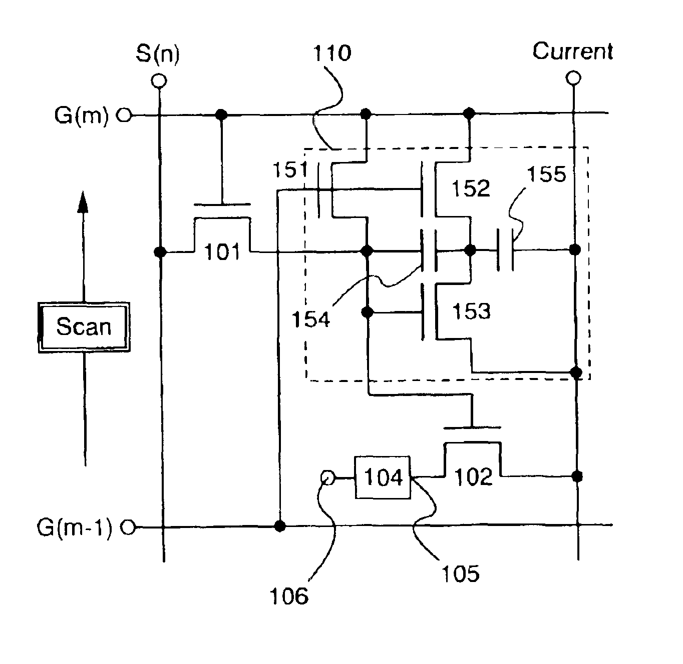
[0090]The structure of a pixel of a voltage compensation circuit of the present invention is shown in FIGS. 1A and 1B. As shown in FIG. 1A, components similar to conventional components are used for a switching TFT 101, a driver TFT 102, an EL element 104, a source signal line (S), a gate signal line (G), and a current supply line (current). The pixel of the present invention has a voltage compensation circuit 110 between an output electrode of the switching TFT 101 and a gate electrode of the driver TFT 102.

[0091]FIG. 1B is a circuit diagram including the structure of the voltage compensation circuit 110. The voltage compensation circuit 110 has a first TFT 151, a second TFT 152, a third TFT 153, a first capacitor 154, and a second capacitor 155. Further, reference symbol G(m) denotes a gate signal line scanned in a number m row, and reference symbol G(m−1) denotes a gate signal line scanned by a number (m−1) row.

[0092]The first capacitor 154 and the second capacitor 155 are arrang...

embodiment mode 2

[0111]FIGS. 25A and 25B show a structure in which a portion differs from the structure of Embodiment Mode 1. As shown in FIG. 25A, components similar to conventional components are used for a switching TFT 2501, a driver TFT 2502, an EL element 2504, a voltage compensation circuit 2510, a source signal line (S(n)), a gate signal line (G(m)), and a current supply line (current).

[0112]FIG. 25B is a circuit diagram including the structure of the voltage compensation circuit 2510. The voltage compensation circuit 2510 has a first TFT 2551, a second TFT 2552, a first capacitive means 2553, and a second capacitive means 2554. The voltage compensation circuit is structured by three TFTs and two capacitors in Embodiment Mode 1, but in Embodiment Mode 2 the voltage compensation circuit 2510 is structured by two TFTs and two capacitors. Further, in FIG. 25B reference symbol G(m) denotes the gate signal line scanned in the number m row, and reference symbol G(m−1) denotes the gate signal line ...

embodiment 1

[Embodiment 1]

[0134]An example of performing SES drive containing an erasure period using a pixel having an added erasure mechanism is explained in Embodiment 1.

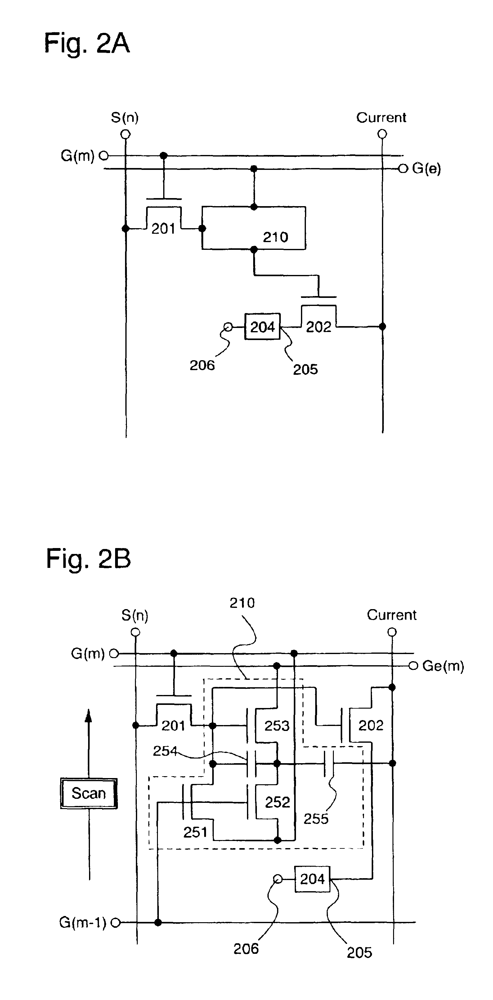
[0135]FIGS. 2A and 2B show structures of a pixel having an erasure mechanism of Embodiment 1. As shown in FIG. 2A, the pixel has a switching TFT 201, a driver TFT 202, an EL element 204, a source signal line (S), a gate signal line (G), and a current supply line (current), which are similar to conventional components, and has a voltage compensation circuit 210 that is similar to the voltage compensation circuit of Embodiment Mode 1. In addition to the gate signal line (G), the pixel also has an erasure gate signal line (Ge) in Embodiment 1. Note that, with respect to the erasure gate signal line (Ge), the normal gate signal line is referred to as a writing gate signal line in Embodiment 1.

[0136]FIG. 2B is a circuit diagram containing the structure of the voltage compensation circuit 210. The voltage compensation circuit 210 ...


PUM

PropertyMeasurementUnit
frame frequencyaaaaaaaaaa
thicknessaaaaaaaaaa
thicknessaaaaaaaaaa

Abstract

A pixel having a structure in which low voltage drive is possible is provided by a simple process. A digital image signal input from a source signal line is input to the pixel through a switching TFT. At this point, a voltage compensation circuit amplifies the voltage amplitude of the digital image signal or transforms the amplitude, and applies the result to a gate electrode of a driver TFT. On-off control of TFTs within the pixel can thus be performed normally even if the voltage of a power source for driving gate signal lines becomes lower.

Description

BACKGROUND OF THE INVENTION[0001]1. Field of the Invention[0002]The present invention relates to a light emitting device. In particular, the present invention relates to a structure of an active matrix light emitting device having thin film transistors (hereafter referred to as TFTs) manufactured on an insulator such as glass or plastic. The present invention also relates to an electronic equipment using the light emitting device in its display portion.[0003]2. Description of the Related Art[0004]The development of display devices in which self light emitting elements such as electro luminescence (EL) elements are used, has been active recently. The term EL element includes either of an element that utilizes luminescence from a singlet exciton (fluorescence), and an element that utilizes luminescence from a triplet exciton (phosphorescence). An EL display device is given as an example of a light emitting device here, but display devices using other self light emitting elements are a...

Claims


Application Information

Patent Timeline
Patent Type & Authority Patents(United States)
IPC IPC(8): G09G3/32G09G3/20G02F1/136
CPCG09G3/3258G09G3/3266G09G3/2022G09G2300/0809G09G2300/0838G09G2300/0842G09G2300/0852G09G2310/0251G09G2320/043G02F1/136
Inventor AZAMI, MUNEHIROTANADA, YOSHIFUMI
Owner SEMICON ENERGY LAB CO LTD
Why Eureka
Try Eureka