Photo-sensor circuit with shutter function and operating method

Inactive Publication Date: 2005-10-25
HONDA MOTOR CO LTD
View PDF3 Cites 16 Cited by
  • Summary
  • Abstract
  • Description
  • Claims
  • Application Information

AI Technical Summary

Benefits of technology

[0014]Accordingly, it is an object of the present invention to provide a method of operation and a photo-sensor circuit capable of initializing a capacitor by turning ON a first transistor before turning ON a second transistor for charging and discharging another capacitor that is a parasitic capacitance of a photodiode PD in order to prevent the first-mentioned capacitor from reproducing an incorrect voltage.
[0015]Another object of the present invention is to provide a photo-sensor circuit wherein a terminal voltage of a parasitic capacitor is always applied to a second capacitor by turning ON a sample-and-hold transistor during the open-state period of a shutter in order to prevent the second capacitor from dropping its voltage.
[0016]A further object of the present invention is to provide a photo-sensor circuit that can generate a pixel signal in a wide dynamic range with high reproducibility, which is achieved by using an initial setting means for executing the logarithmic operation by changing a power supply voltage in addition to a shutter function.

Problems solved by technology

This results in decreasing the reproducibility of the signal.
However, there arises such a problem that a charge of the capacitor C2 becomes smaller than a charge of the capacitor C1.

Method used


Image

  • Photo-sensor circuit with shutter function and operating method
  • Photo-sensor circuit with shutter function and operating method
  • Photo-sensor circuit with shutter function and operating method

Examples


Embodiment Construction

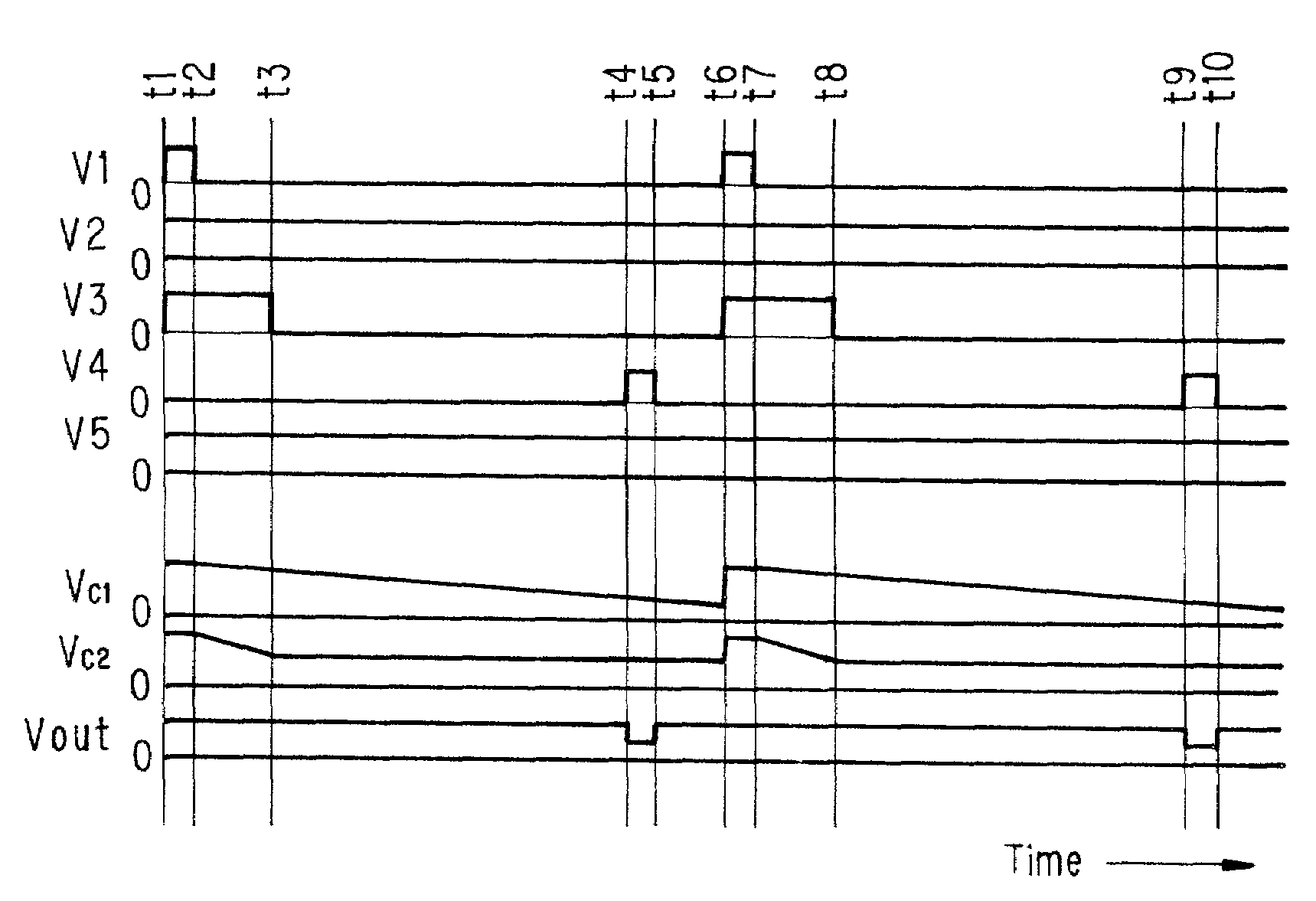
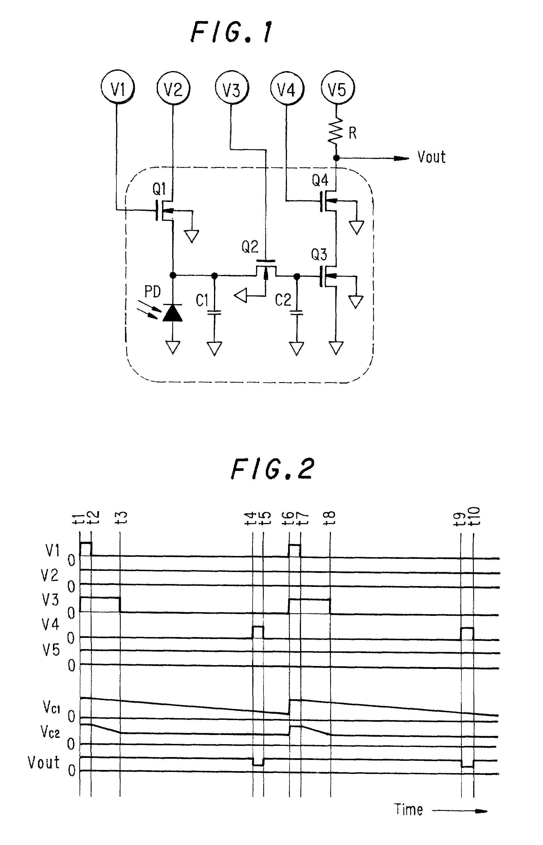
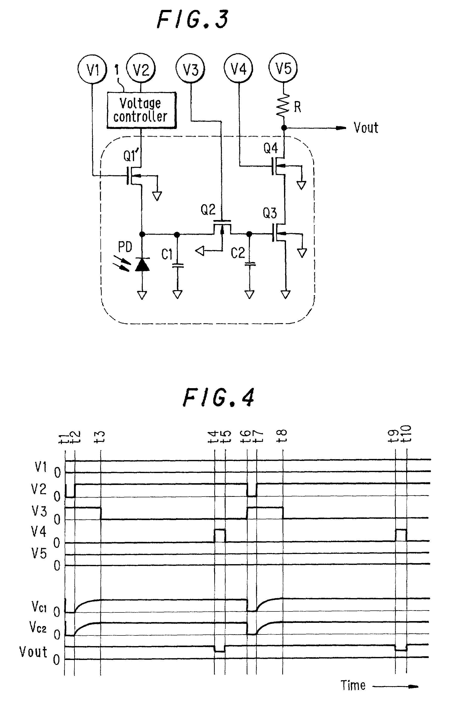
[0030]Referring to FIG. 1, a photo-sensor circuit according to an embodiment of the present invention comprises a photodiode PD being a light-detecting element for sensing light and converting it into an electric signal, a MOS transistor Q1 for charging and discharging a capacitor C1 being a parasitic capacitance of the photodiode PD, a capacitor C2 for accumulating therein a terminal voltage of the photodiode PD as a pixel signal, a MOS transistor Q2 for transferring an electric charge of the capacitor C1 to a capacitor C2, a MOS transistor Q3 for amplifying a terminal voltage of the capacitor C2 and a MOS transistor Q4 for selectively outputting the amplified pixel signal.

[0031]In the above photo-sensor circuit of FIG. 1 according to the present invention, an electric signal corresponding to a light signal is obtained by applying control signals for driving respective components of the circuit in a new and inventive method.

[0032]Namely, as shown in FIG. 2, the transistor Q1 is tur...


PUM


Abstract

A photo-sensor circuit according to an embodiment of the present invention comprises a photo-detecting element (PD) for detecting a light signal and converting the same signal into an electric signal, a first MOS transistor (QT) for charging and discharging parasitic capacitance (C1), a capacitor (C2) for accumulating a terminal voltage of the photo-detecting element as a pixel signal, a second MOS transistor (Q2) for transferring a parasitic capacitance charge from the photo-detecting element to the capacitor (C2), a third MOS transistor (Q3) for amplifying the terminal voltage of the capacitor and a fourth MOS transistor (Q4) for selectively outputting an amplified pixel signal. In the above structure, the first MOS transistor and the second MOS transistor are turned ON for a certain period of time before accumulation of a pixel signal to equalize terminal voltages of the photo-detecting element and the capacitor by charging and discharging the parasitic capacitance of the photo-detecting element and the capacitor, the second MOS transistor is turned OFF and the capacitor is open after a certain period of time of accumulation of the pixel signal and then the fourth MOS transistor is switched ON. This photo-sensor circuit offers an advantageous feature of producing a pixel signal having high reproducibility.

Description

BACKGROUND OF THE INVENTION[0001]The present invention relates to a photo-sensor circuit for detecting a light signal and converting the detected light signal into an electric signal and a method of operating the circuit, and, more specifically, to a photo-sensor circuit having a shutter function.[0002]FIG. 1 shows a photo-sensor circuit having a shutter function (sample-and-hold function), which can be used as one of pixel detecting elements composing an image sensor. This photo-sensor circuit comprises a photodiode PD for detecting a light signal and converting it into an electric signal, a MOS transistor Q1 for charging / discharging a capacitor C1 being a parasitic capacitance of the photodiode, a capacitor C2 for accumulating a terminal voltage of the photodiode PD as a pixel signal, a MOS transistor Q2 for transferring an electric charge from the capacitor C1 to the capacitor C2, a MOS transistor Q3 for amplifying a terminal voltage of the capacitor C2 and a MOS transistor Q4 fo...

Claims


Application Information

Patent Timeline
IPC IPC(8): G01J1/46H01L27/146H04N1/028H04N5/335H04N5/341H04N5/353H04N5/355H04N5/357H04N5/369H04N5/374H04N5/3745H04N5/376H04N5/378
CPCG01J1/46
Inventor SHINOTSUKA, SUKEYUKITAKEBE, KATSUHIKO
Owner HONDA MOTOR CO LTD
Why Eureka
Try Eureka