Process and mask projection system for laser crystallization processing of semiconductor film regions on a substrate

a projection system and laser crystallization technology, applied in the field of semiconductor film processing techniques, can solve problems such as damage to and achieve the effect of increasing the lifetime of the optics of the system and reducing energy

Inactive Publication Date: 2005-11-01
THE TRUSTEES OF COLUMBIA UNIV IN THE CITY OF NEW YORK
View PDF129 Cites 60 Cited by
  • Summary
  • Abstract
  • Description
  • Claims
  • Application Information

AI Technical Summary

Benefits of technology

[0007]One of the objects of the present invention is to provide an improved projection irradiation system and process to implement the sequential lateral solidification. Another object of the present invention is to provide a system and process using which, the mask of utilized for shaping...

Problems solved by technology

This is problematical when processes requiring high fluence on the substrate 10 are considered, as the high energy density incident on...

Method used


Image

  • Process and mask projection system for laser crystallization processing of semiconductor film regions on a substrate
  • Process and mask projection system for laser crystallization processing of semiconductor film regions on a substrate
  • Process and mask projection system for laser crystallization processing of semiconductor film regions on a substrate

Examples


Embodiment Construction

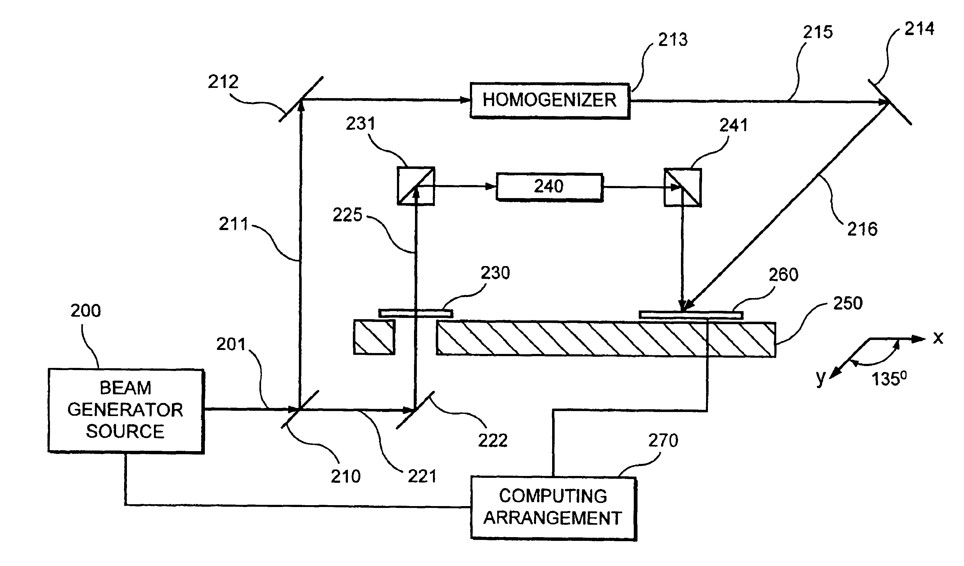
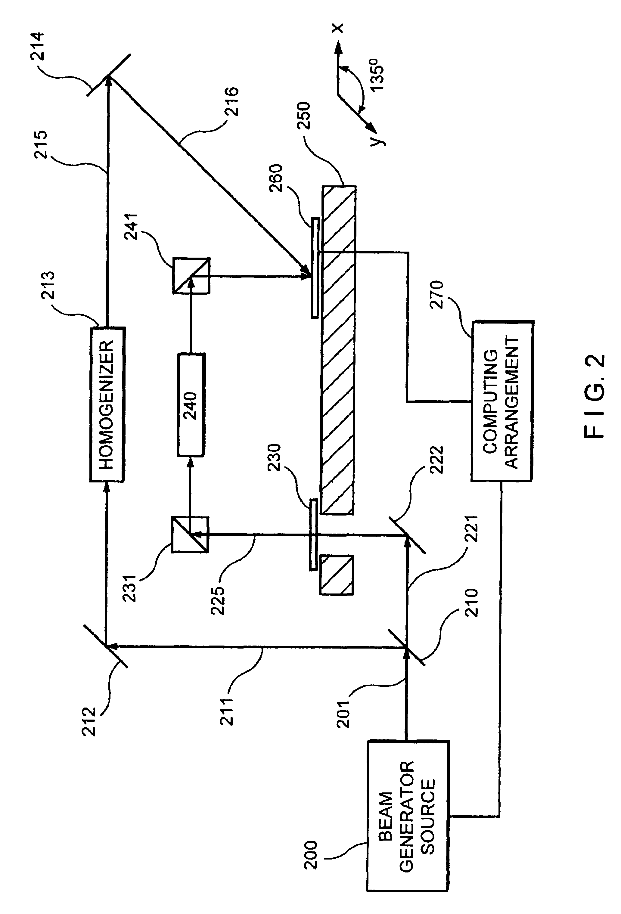
[0025]An exemplary embodiment of a projection irradiation system according to the present invention is shown as a schematic block diagram in FIG. 2. In particular, a beam source 200 (e.g., a pulsed excimer laser) generates an excimer laser beam 201 (composed of beam pulses) which passes through a beam splitter 210 to become two beams 211, 221. In one exemplary implementation of the present invention, these two split beams 211, 221 may each have 50% of the energy that of the original beam 201. It is within the scope of the present invention to possibly utilize other energy combinations with the exemplary system of the present invention illustrated in FIG. 2. Each of the beams 211, 221 is composed of a set of beam pulses.

[0026]The first split beam 211 can be redirected by a mirror 212 toward a homogenizer 213, which then outputs a homogenized beam 215. Thereafter, the homogenized beam 215 (and its respective beam pulses) can be redirected by a second mirror 214 so as to be incident on...


PUM

PropertyMeasurementUnit
Timeaaaaaaaaaa
Thicknessaaaaaaaaaa
Transparencyaaaaaaaaaa

Abstract

A process and system for processing a silicon thin film on a sample are provided. In particular, an irradiation beam generator is controlled to emit irradiation beam pulses at a predetermined repetition rate. These irradiation beam pulses are then separated into a first set of beam pulses and a second set of beam pulses. The first set of beam pulses are caused to irradiate through a mask to produce a plurality of beamlets. The second set of beam pulses and the beamlets are caused to impinge and irradiate at least one section of the silicon thin film. When the second set of beam pulses and the beamlets simultaneously irradiate the section of the silicon thin film, this combination of the beamlets and second set of beam pulses provides a combined intensity which is sufficient to melt the section of the silicon thin film throughout an entire thickness of the section.

Description

CROSS-REFERENCE TO RELATED APPLICATIONS[0001]This application is a national stage application of PCT Application No. PCT / US01 / 44415 which was filed on Nov. 27, 2001 and published in English on May 30, 2002 as International Publication No. WO 02 / 42847 (the “International Application”). This application claims priority from the International Application pursuant to 35 U.S.C. §365. The present application also claims priority under 35 U.S.C. §119 from U.S. patent application Ser. No. 60 / 253,256 filed Nov. 27, 2000. The entire disclosures of these applications are incorporated herein by reference.NOTICE OF GOVERNMENT RIGHTS[0002]The U.S. Government has certain rights in this invention pursuant to the terms of the Defense Advanced Research Project Agency award number N6600198-1-8913.FIELD OF THE INVENTION[0003]The present invention relates to techniques for processing of semiconductor films, and more particularly to techniques for processing semiconductor films using patterned laser beam...

Claims


Application Information

Patent Timeline
IPC IPC(8): G03B27/42B23K26/06B23K26/067H01L21/20H01L21/268H01L21/768H01S3/00
CPCB23K26/0604B23K26/0608B23K26/063B23K26/0656B23K26/067G03B27/42H01L21/2026H01L21/76894B23K26/0622B23K26/066H01L21/02532H01L21/02678H01L21/02686H01L21/02691G03F7/20
Inventor IM, JAMES S.
Owner THE TRUSTEES OF COLUMBIA UNIV IN THE CITY OF NEW YORK
Why Eureka
Try Eureka