Integrated circuit insulator and method

Inactive Publication Date: 2005-11-08
TEXAS INSTR INC
View PDF4 Cites 4 Cited by
  • Summary
  • Abstract
  • Description
  • Claims
  • Application Information

AI Technical Summary

Benefits of technology

[0006]The present invention provides a planarizing two-stage deposition of premetal dielectric with plasma enhancement: a first low bias deposition to eliminate charge buildup and / or physical damage of transistor gate dielectric followed by a second high bias deposition for planarization.

Problems solved by technology

These approaches have problems including the multiple steps required for fabrication of the insulating layer and gate dielectric breakdown from gate exposure to a plasma during PECVD TEOS used for premetal dielectric.

Method used


Image

  • Integrated circuit insulator and method
  • Integrated circuit insulator and method
  • Integrated circuit insulator and method

Examples


Embodiment Construction

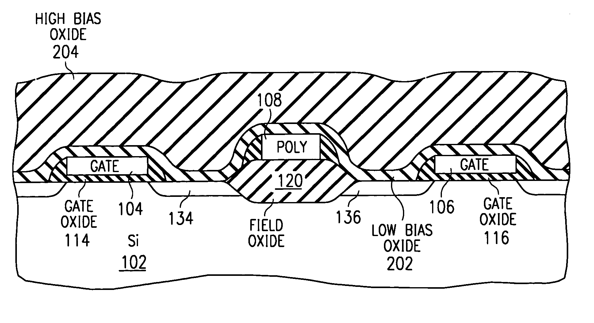
[0014]First Preferred Embodiment

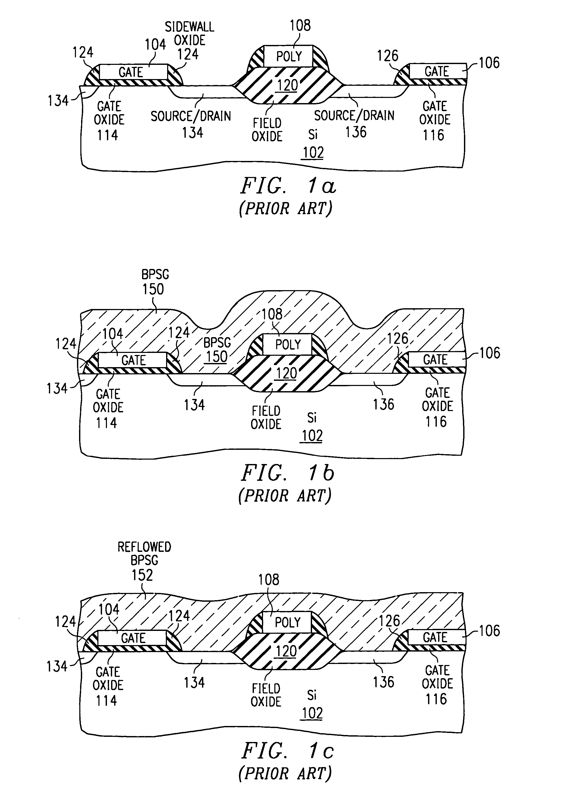
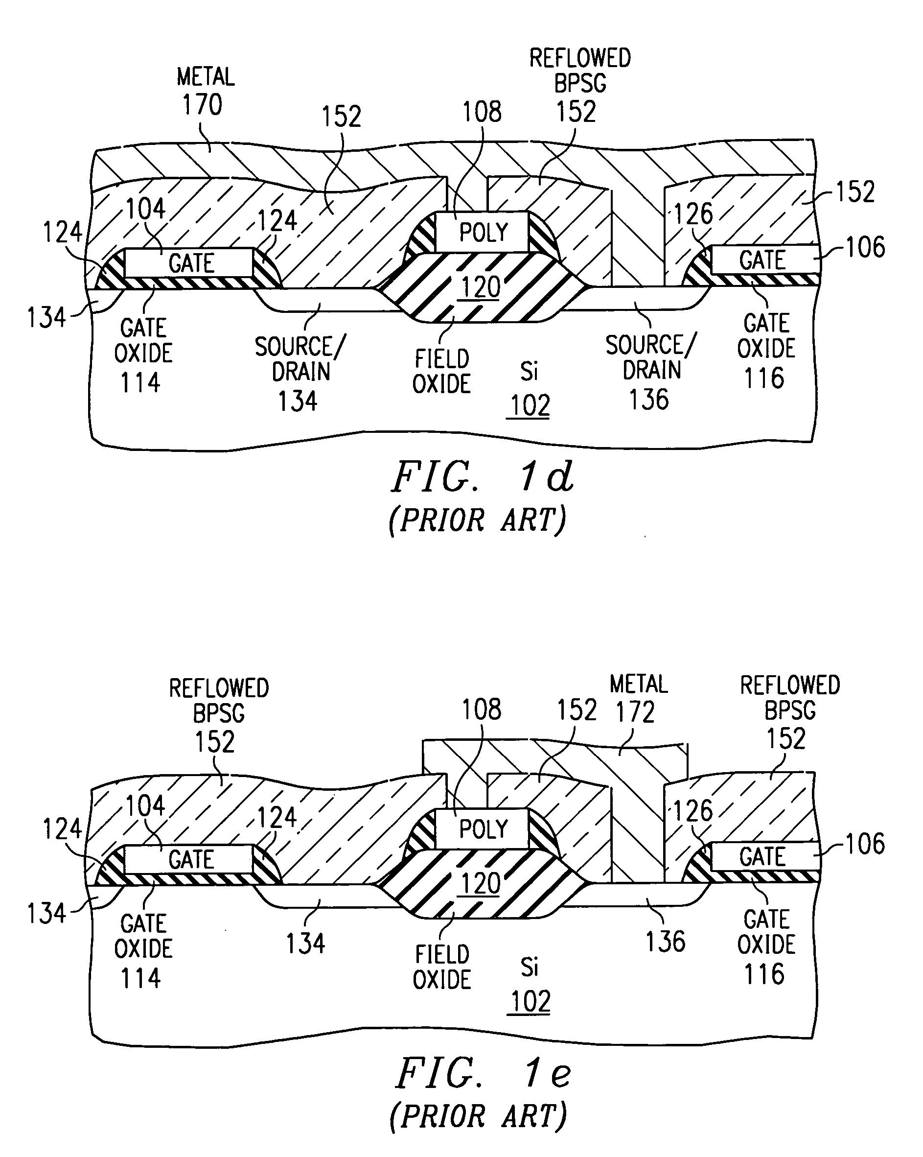
[0015]To order to explain the first preferred embodiment premetal dielectric layer fabrication, first consider a known method of fabrication. In particular, FIG. 1a shows in cross sectional elevation view a portion of a silicon substrate 102 with polysilicon gates 104–106 on gate insulator silicon dioxide (gate oxide) 114–116 and having sidewall oxides 124–126 for alignment of source / drains 134–136 and with the transistors separated by field oxide 120 with polysilicon line 108 running over field oxide 120. Typically, the polysilicon gates and the field oxide extend about 0.3 μm above the substrate surface, so the top of polysilicon line 108 lies about 0.6 μm above the substrate surface. Gate oxide 114–116 may be about 6 nm thick. A somewhat planar insulating layer to cover the gates and field oxide then can be formed as follows. First, deposit layer 150 of borophosphosilicate glass (BPSG, roughly 5% boron and 5% phosphorus) about 1 μm thick by plasma ...


PUM


Abstract

A two-stage plasma enhance dielectric deposition with a first stage of low capacitively-coupled RF bias with conformal deposition (202) followed by high capacitively-coupled RF bias for planarizing deposition (204) limits the charge build up on the underlying structure (104, 106, 108).

Description

CROSS-REFERENCE TO RELATED APPLICATIONS[0001]This application is a divisional of patent application Ser. No. 08 / 692,887, filed Aug. 1, 1996, now abandoned.BACKGROUND OF THE INVENTION[0002]The invention relates to semiconductor devices, and, more particularly, to integrated circuit insulation and methods of fabrication.[0003]Integrated circuits typically include field effect transistors with source / drains formed in a silicon substrate and insulated gates on the substrate plus multiple overlying metal (or polysilicon) interconnection levels with an insulating layer between the gates / sources / drains and the first metal level (premetal dielectric) and between successive metal levels (intermetal-level dielectric). Vertical vias in the insulating layers filled with metal (or polysilicon) provide connections between adjacent metal levels and between the gate / source / drain and the first metal level. Each insulating layer must cover the relatively bumpy topography of a metal level or the gates...

Claims


Application Information

Patent Timeline
IPC IPC(8): H01L21/02H01L21/316H01L21/768
CPCH01L21/02131H01L21/02164H01L21/022H01L21/02274H01L21/31612H01L21/31629H01L21/76801
Inventor NAG, SOMNATH S.DIXIT, GIRISH A.KRISHNAN, SRIKANTH
Owner TEXAS INSTR INC
Why Eureka
Try Eureka