Noise-reducing arrangement and method for signal processing

a signal processing and noise reduction technology, applied in the field of signal communication, can solve problems such as current problems, circuitry denigration of the performance of sensitive analog circuits, and communication systems including high-speed digital signal processors. achieve the effect of enhancing noise problems and reducing effective nois

Inactive Publication Date: 2005-11-08
THE BOARD OF TRUSTEES OF THE LELAND STANFORD JUNIOR UNIV
View PDF42 Cites 144 Cited by
  • Summary
  • Abstract
  • Description
  • Claims
  • Application Information

AI Technical Summary

Benefits of technology

[0010]Various implementations of the present invention reduce the effective noise by causing the analog and digital portions of the system to function during separate time intervals. According to certain embodiments, the noise-generating portions of the system are turned off while the analog block operates. The data acquired during this period is stored for subsequent processing by the digital portion. This technique is applicable to systems in which part of the incoming signal may be disregarded without significant degradation in performance of the rest of the system. It is also advantageous in situations where other design considerations, such as cost or power consumption, enhance the noise problem.

Problems solved by technology

Such communication systems including these high-speed digital signal processors have encountered a serious noise problem when attempting to implement the analog circuitry nearby the digital signal processing circuitry.
The noise generated by digital signal processing circuitry has denigrated the performance of sensitive circuits in the analog circuitry.
This problem is being currently encountered by receiver circuitry for the Global Position System (GPS).
Unfortunately, a major design issue in mixed-signal systems of this type is the adverse effect of digital switching noise coupled through the substrate to sensitive analog circuits.

Method used


Image

  • Noise-reducing arrangement and method for signal processing
  • Noise-reducing arrangement and method for signal processing
  • Noise-reducing arrangement and method for signal processing

Examples


Embodiment Construction

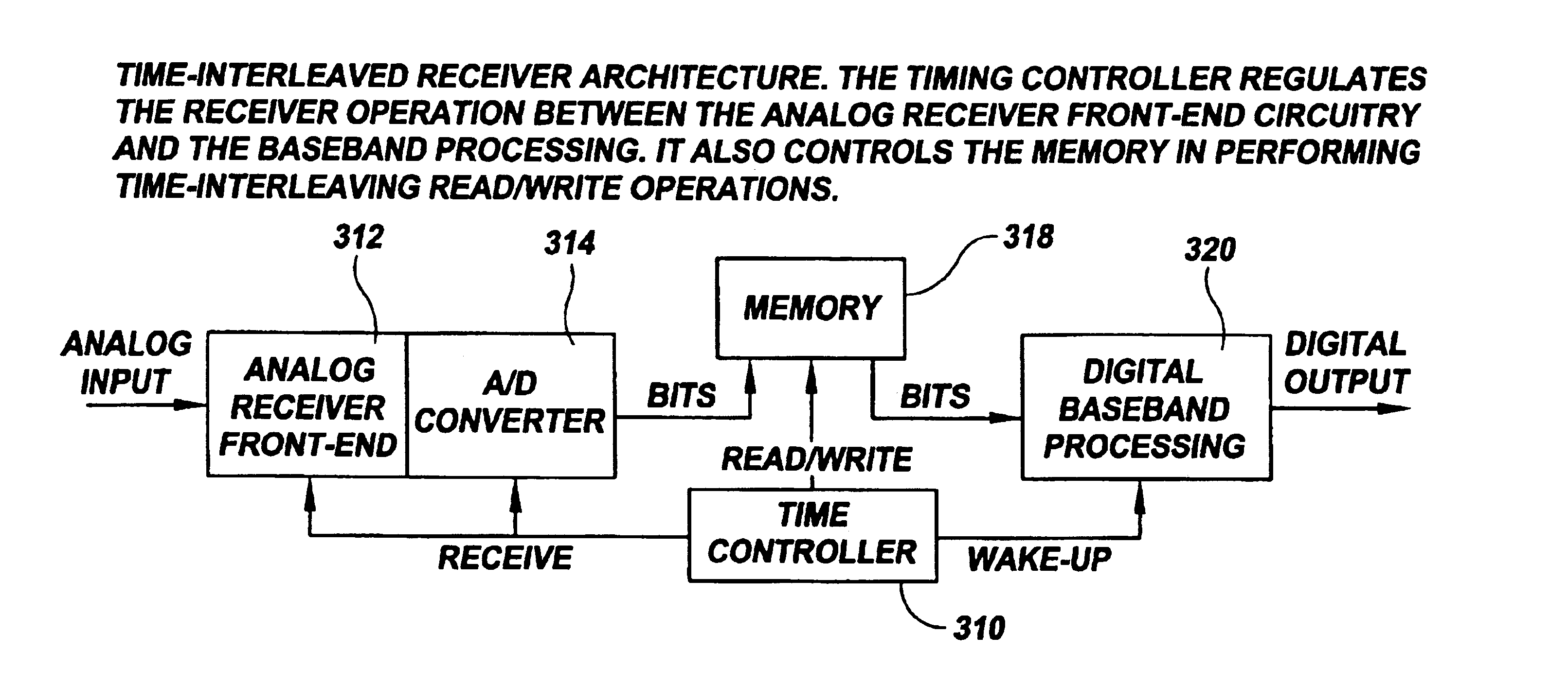
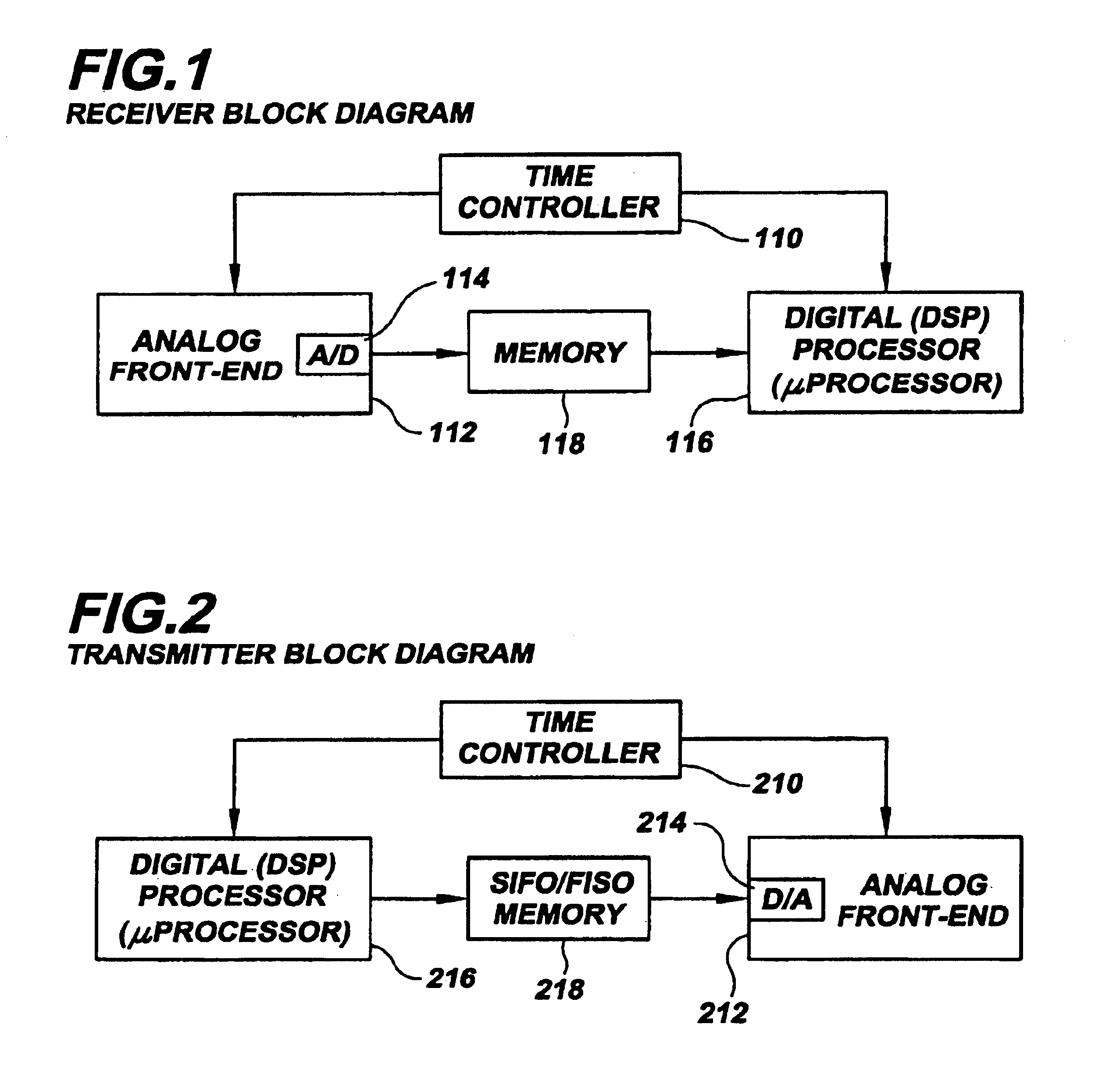
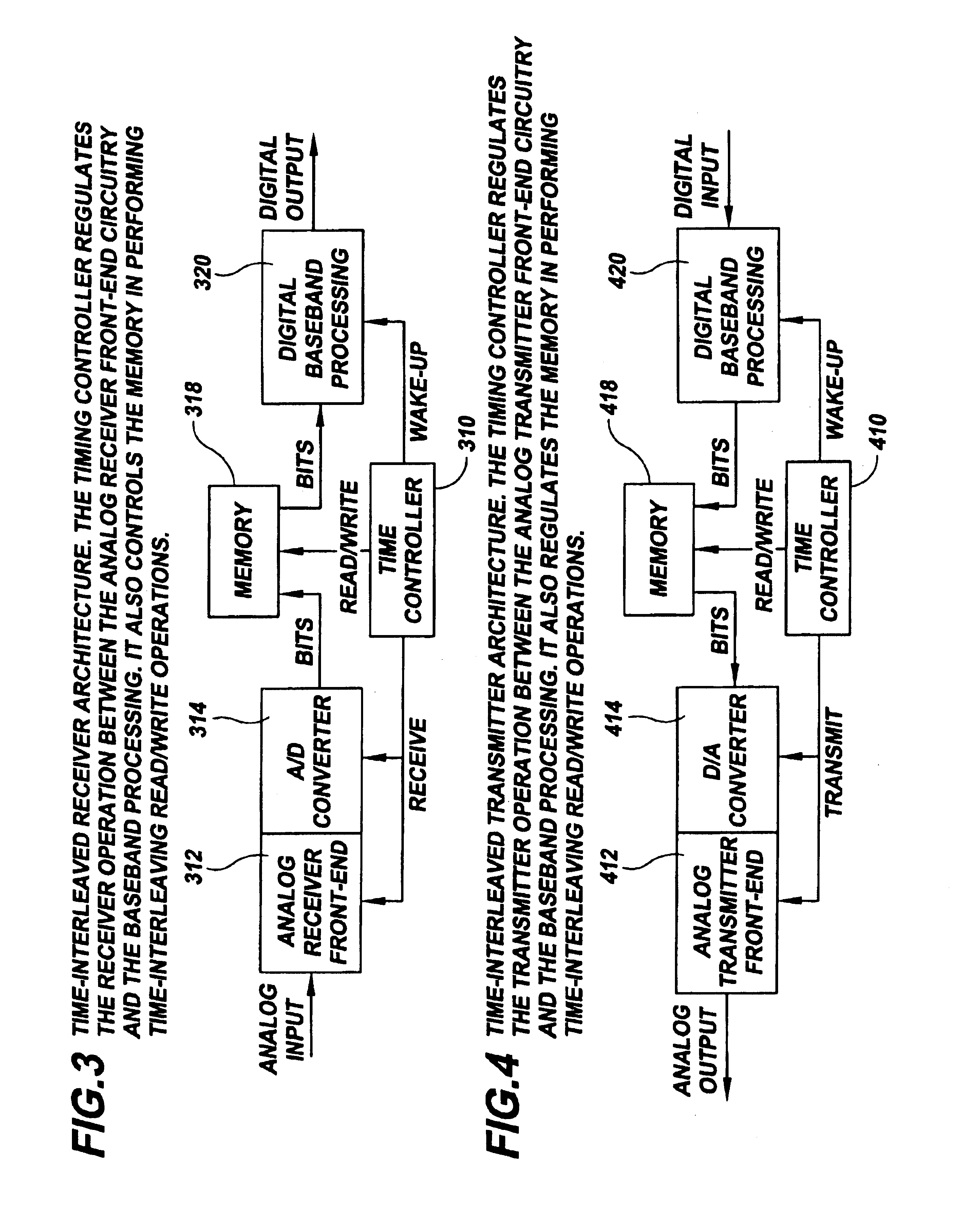
[0027]The present invention is believed to be applicable to a variety of systems and arrangements that process data using both analog and digital processing circuitry. The present invention has been found to be particularly advantageous for systems in which part of the incoming data signal may be disregarded without significant degradation in system performance and / or where cost or power consumption is of concern, or in which the timing control of the analog and digital sections of a circuit can be implemented without loss of analog data. An appreciation of the invention may be ascertained through a discussion in the context of such system applications.

[0028]In a typical application of the present invention, a communication arrangement includes both analog circuitry and digital signal processing circuitry for communicating data. The analog circuitry couples to the digital circuitry using conventional analog-digital or analog-digital conversion circuitry. In certain implementations o...


PUM


Abstract

A communication system uses analog and digital circuits along the same data path in a manner that permits the analog circuitry to avoid adverse affects caused by the digital circuitry. Consistent with one embodiment directed to a signal processing system that detects faint incoming signals, the analog and digital circuits are implemented on a single piece of silicon. In such signal processing systems, noise generated by digital processing blocks can degrade the performance of sensitive analog portions. The effective noise is reduced by causing the analog and digital portions of the system to function during separate time intervals. The noise-generating portions of the system may then be turned off during a first data-communication interval while the analog block operates. The data acquired during this period is stored for subsequent processing by the digital portion during a second shorter data-communication interval. Other aspects are applicable to reception arrangements in which part of the incoming signal may be disregarded without significant degradation in performance of the rest of the system, and other aspects are directed to transmission arrangements in which the inverse of the above reception arrangement is used.

Description

RELATED PATENT DOCUMENTS[0001]This application claims the benefit of U.S. Provisional Application Ser. No. 60 / 102,865, filed on Oct. 2, 1998, and entitled “Noise-Reducing Arrangement And Method For Signal Processing.”BACKGROUND STATEMENTS[0002]Inventive aspects disclosed herein were made with Government support under contract N65236-96-C-8608. The Government has certain rights in these inventive aspects.BACKGROUND STATEMENTS[0003]Inventive aspects disclosed herein were made with Government support under contract N65236-96-C-8608. The Government has certain rights in these inventive aspects.FIELD OF THE INVENTION[0004]The present invention relates generally to signal communication. More particularly, the present invention relates to signal communication involving digital signal processing circuitry operating at speeds that generate noise sufficient to adversely affect nearby analog circuitry that is processing the same data.BACKGROUND OF THE INVENTION[0005]Many signal processing syst...

Claims


Application Information

Patent Timeline
Patent Type & Authority Patents(United States)
IPC IPC(8): H04B1/10H04B1/04H04B1/30
CPCH04B1/0475H04B1/30
Inventor SHAEFFER, K. DEREKMENG, THERESA H.LEE, THOMAS H.READER, SYDNEY
Owner THE BOARD OF TRUSTEES OF THE LELAND STANFORD JUNIOR UNIV
Why Eureka
Try Eureka