Low cost substrate for an integrated circuit device with bondpads free of plated gold

a technology of bondpads and integrated circuits, which is applied in the direction of non-metallic protective coating applications, printed circuit aspects, and the improvement of the adhesion of the insulating substrate, etc., can solve the problems of device failure, oxidation, and the material typically used for the bondpad, for example copper

Inactive Publication Date: 2005-11-29
TEXAS INSTR INC
View PDF34 Cites 14 Cited by
  • Summary
  • Abstract
  • Description
  • Claims
  • Application Information

AI Technical Summary

Problems solved by technology

For example, the packaging cost can easily exceed the cost of the IC chip itself.
In addition, many of the device failures that occur are generally packaging related.
Unfortunately, the material typically used for the bondpads, for example, copper, oxidizes when remaining exposed throughout the assembly process, until the bondpads are soldered.
Oxidation on the surface of the bondpads, as well as contaminants that may gather on the bondpad surface when exposed during the assembly process, often detrimentally affect the metallurgical bond between the bondpads and the corresponding traces on the PCB.
Specifically, the dielectric nature of the oxidation may affect the electrical connection between the two, while in some cases also affecting the strength of the bond used to hold the IC package to the PCB.
Problems with the electrical connections between the bondpads on the packages and PCBs, as well as the strength of the mechanical bond between the two, can often affect the overall operation and longevity of the assembly.

Method used


Image

  • Low cost substrate for an integrated circuit device with bondpads free of plated gold
  • Low cost substrate for an integrated circuit device with bondpads free of plated gold
  • Low cost substrate for an integrated circuit device with bondpads free of plated gold

Examples


Embodiment Construction

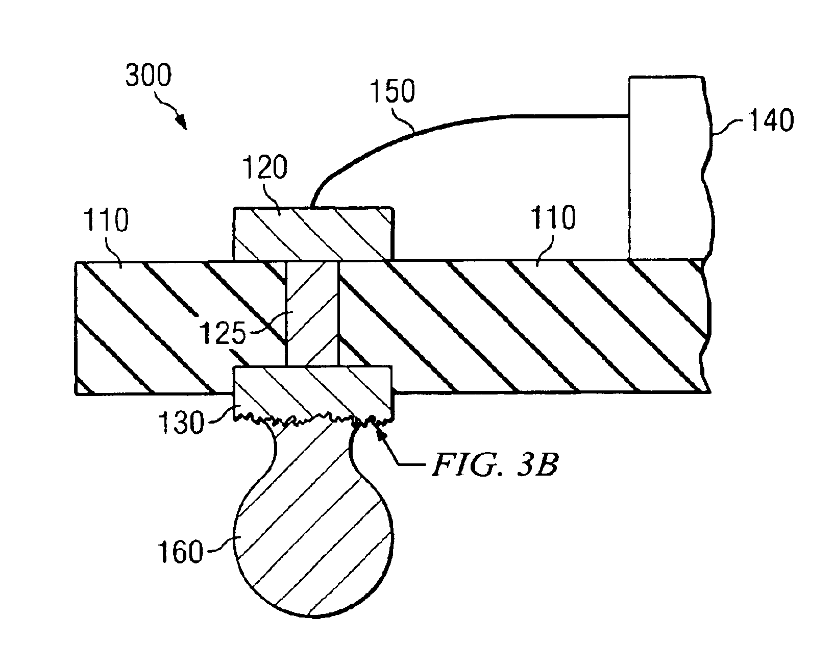
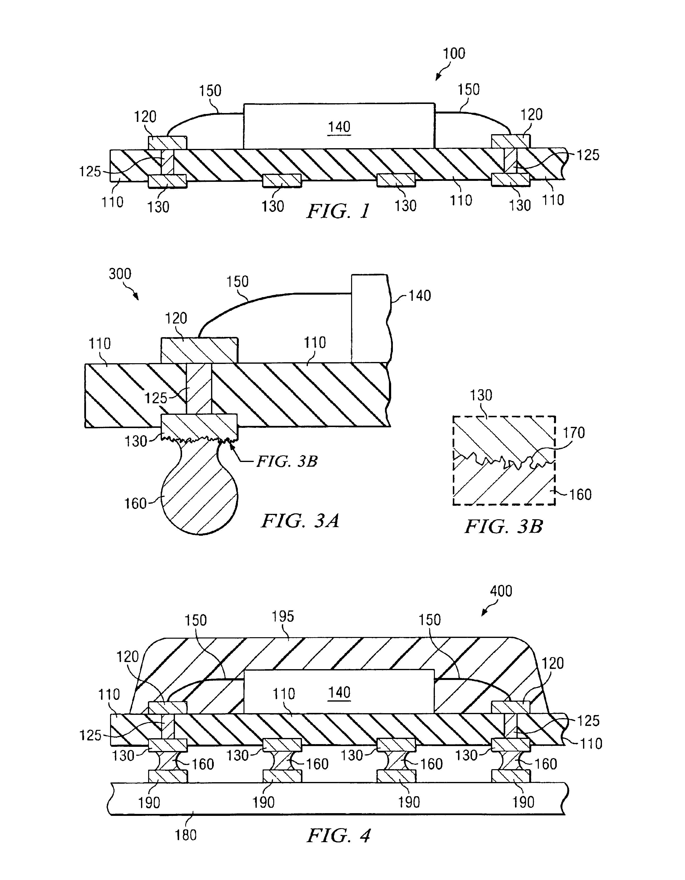
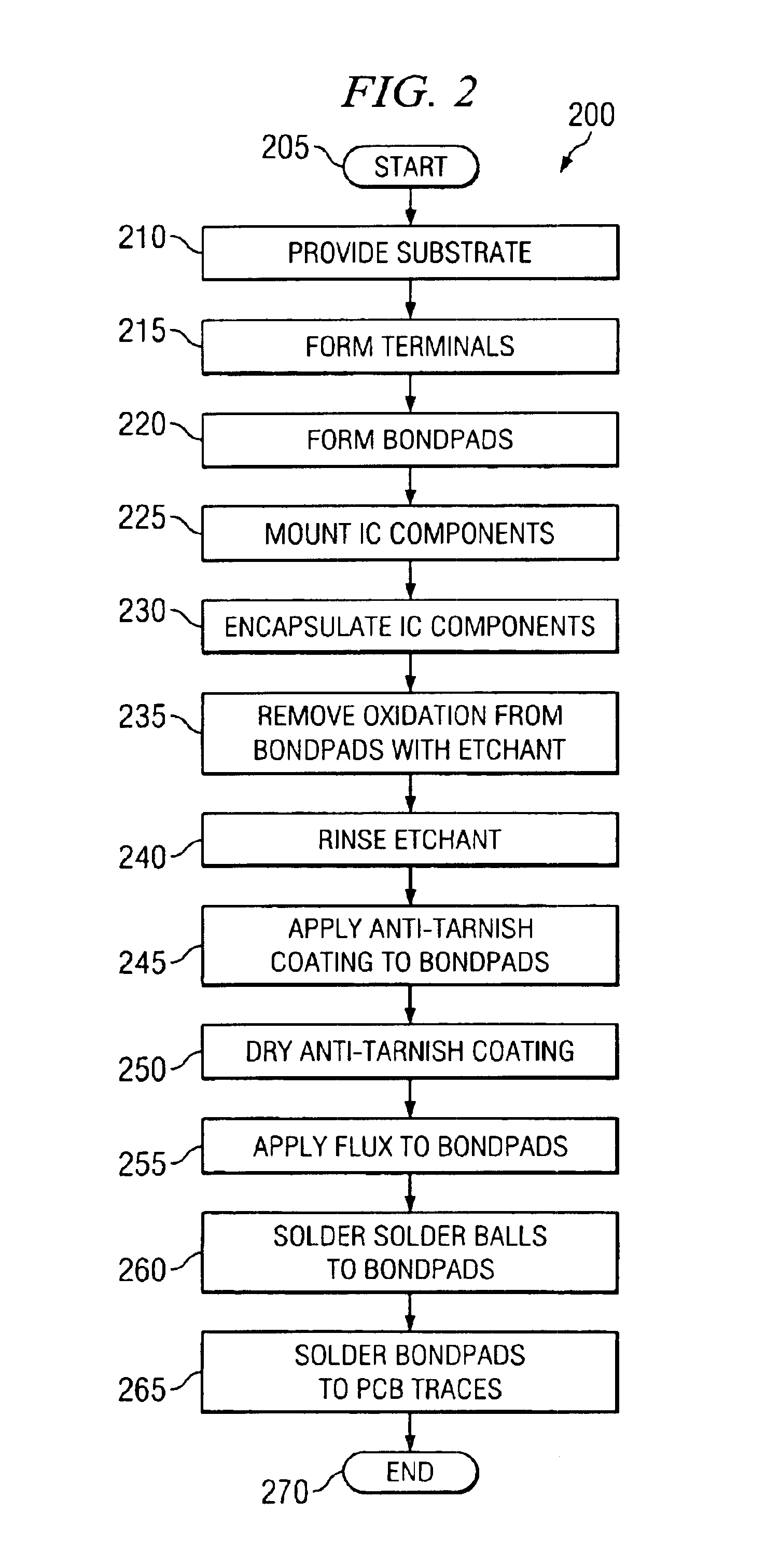
[0014]Referring initially to FIG. 1, illustrated is a side view of one embodiment of an integrated circuit (IC) assembly 100 shown during a manufacturing process conducted according to the principles disclosed herein. The assembly 100 includes a package substrate 110, which may be formed from any appropriate dielectric material. In addition, the substrate 110 may include multiple layers for forming various electrical interconnects, and may be constructed using conventional techniques.

[0015]The IC assembly 100 further includes multiple electrical terminals (one of which is labeled 120) formed on a first side of the substrate 110. In an advantageous embodiment, the terminals 120 may be formed from copper, and may be electrically connected through the substrate 110 using vias 125. The IC assembly 100 further includes a plurality of package bondpads (one of which is labeled 130) formed on the second side of the substrate 110. As illustrated, various ones of the bondpads 130 are electric...


PUM


Abstract

Disclosed herein is a process for assembling an integrated circuit, as well as the assembly resulting from the process, employing a surface treatment of bondpad surfaces. In one aspect, a method of assembling an integrated circuit includes providing a substrate having electrical terminals on a first side of the substrate and a bondpad on a second side of the substrate opposing the first side. In this embodiment, the bondpad is electrically coupled to at least one of the terminals on the first side. In addition, the method includes mounting an integrated circuit chip to the first side of the substrate, where the integrated circuit component has a lead adapted to be wire-bonded to the terminal. The method further includes removing oxidation from the bondpad, where the bondpad is adapted to be metallurgically bonded to a trace on a printed circuit board. Moreover, this embodiment of the method includes metallurgically bonding the bondpad to the trace.

Description

CROSS-REFERENCE TO RELATED APPLICATION[0001]This Application claims the benefit of U.S. Provisional Application Ser. No. 60 / 483,457, filed on Jun. 27, 2003, which is commonly assigned with the present Application and incorporated herein by reference for all purposes.TECHNICAL FIELD[0002]Disclosed embodiments relate generally to integrated circuits, and more particularly to methods for assembling integrated circuit assemblies, as well as the resulting integrated circuit assemblies, by employing a surface treatment on bondpad surfaces prior to soldering terminals to the bondpads.BACKGROUND[0003]Integrated circuits (ICs) are usually formed on semiconductor wafers. The wafers are separated into individual dies or chips, and the individual chips are then handled and packaged. The packaging process is one of the most critical steps in the IC fabrication process, both from the point of view of cost and of reliability. For example, the packaging cost can easily exceed the cost of the IC chi...

Claims


Application Information

Patent Timeline
Patent Type & Authority Patents(United States)
IPC IPC(8): H01L21/44H01L21/48H01L21/50H01L23/50H05K3/28H05K3/34H05K3/38
CPCH05K3/3489H01L2224/48227H01L2924/01078H01L2924/01079H01L2924/14H05K3/282H05K3/3457H05K3/383H05K2201/10734H01L2924/01019
Inventor ESTEPA, ERWIN R.MEDINA, JOEL T.AZURIN, MARIA ALESSSANDRAANO, KAZUAKI
Owner TEXAS INSTR INC
Why Eureka
Try Eureka