Versatile system for triple-gated transistors with engineered corners

a technology of engineered corners and transistors, applied in the field of semiconductor devices, can solve the problems of reducing reducing the cost of the device, and generating numerous challenges to the semiconductor manufacturing process, and achieving the effects of improving the efficiency of the device, and improving the reliability of the devi

Active Publication Date: 2005-11-29
TEXAS INSTR INC
View PDF7 Cites 7 Cited by
  • Summary
  • Abstract
  • Description
  • Claims
  • Application Information

AI Technical Summary

Benefits of technology

[0013]The present invention provides a versatile system, comprising a number of apparatus and methods, for producing multiple-gated transistor structures having selectively engineered corners and edges. Certain performance and reliability concerns commonly associated with conventional methods are obviated by structures according to the present invention. Comprehending the increased costs associated with SOI-based methods, the system of the present invention is readily implemented in or adaptable to a wide variety of commercially viable fabrication technologies. The system of the present invention thus overcomes a number of difficulties inherent in conventional approaches while optimizing device performance and reliability in an easy, efficient and cost-effective manner.
[0014]The present invention recognizes that, during the formation and processing of certain semiconductor device structures, it may be necessary to tailor targeted portions of a single structure, without altering the remainder of that structure. This is especially true of silicon body structures utilized in the formation multiple-gate transistors. For a number of structural, performance and reliability reasons, it may be desirable to blunt or otherwise nullify square corners or edges along the upper portion of a silicon body structure (i.e., the portion of the structure opposite the silicon bulk). Such an approach should greatly reduce or eliminate, however, any blunting or rounding of corners or edges along the lower portion of the silicon body structure.

Problems solved by technology

The increased packing density of the integrated circuit generates numerous challenges to the semiconductor manufacturing process.
Unfortunately, most conventional fabrication processes (e.g., lithography) are limited in their ability to reliably produce transistor features of extremely small dimension.
In addition to fabrication process limitations, performance limitations are also a barrier to significant reductions in planar transistor gate lengths.
Typically, reduced gate length can result in short channel effects that degrade transistor performance.
In short channel devices, however, the channel region is also affected by source and drain voltages—causing an increased off-state current, due to VT roll-off, decreased sub-threshold slope, and degraded output current.
Although such approaches are capable of producing multiple gate devices that offer improved performance over planar transistor designs, a number of production, performance and reliability issues still preclude their commercial viability in high-volume semiconductor fabrication.
SOI wafers tend to be significantly more expensive than ordinary silicon substrates.
Considerable overhead is added to fabrication processes by the etching processes involved in forming channel structures.
Furthermore, channel surfaces exposed to the etch processes can incur damage that degrades their structural and electrical integrity throughout the lifetime of the device.
Even if etch processes successfully form a channel structure, the physical form of the resulting channel structure may inherently cause a number of problems.
Sharp angles within semiconductor structures introduce structural discontinuities and instabilities (e.g., lattice structure instability) to those structures.
Unfortunately, most such approaches have no way to selectively round only the upper edges of the channel block.
This creates a number of performance problems, and complicates subsequent processing steps.

Method used


Image

  • Versatile system for triple-gated transistors with engineered corners
  • Versatile system for triple-gated transistors with engineered corners
  • Versatile system for triple-gated transistors with engineered corners

Examples


Embodiment Construction

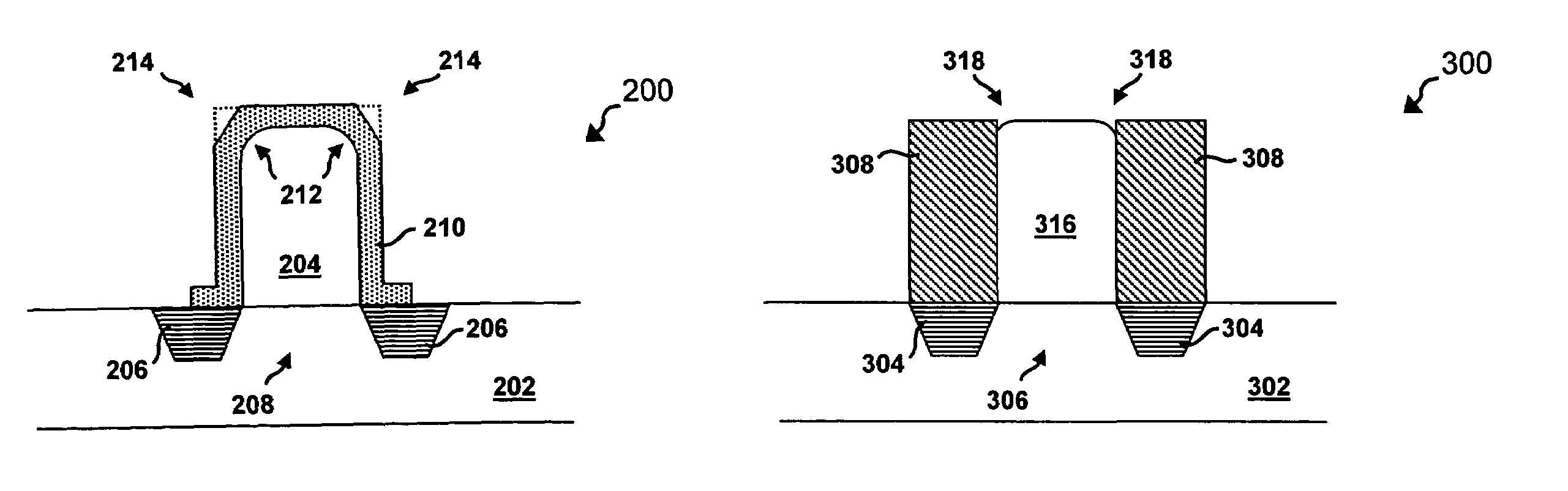
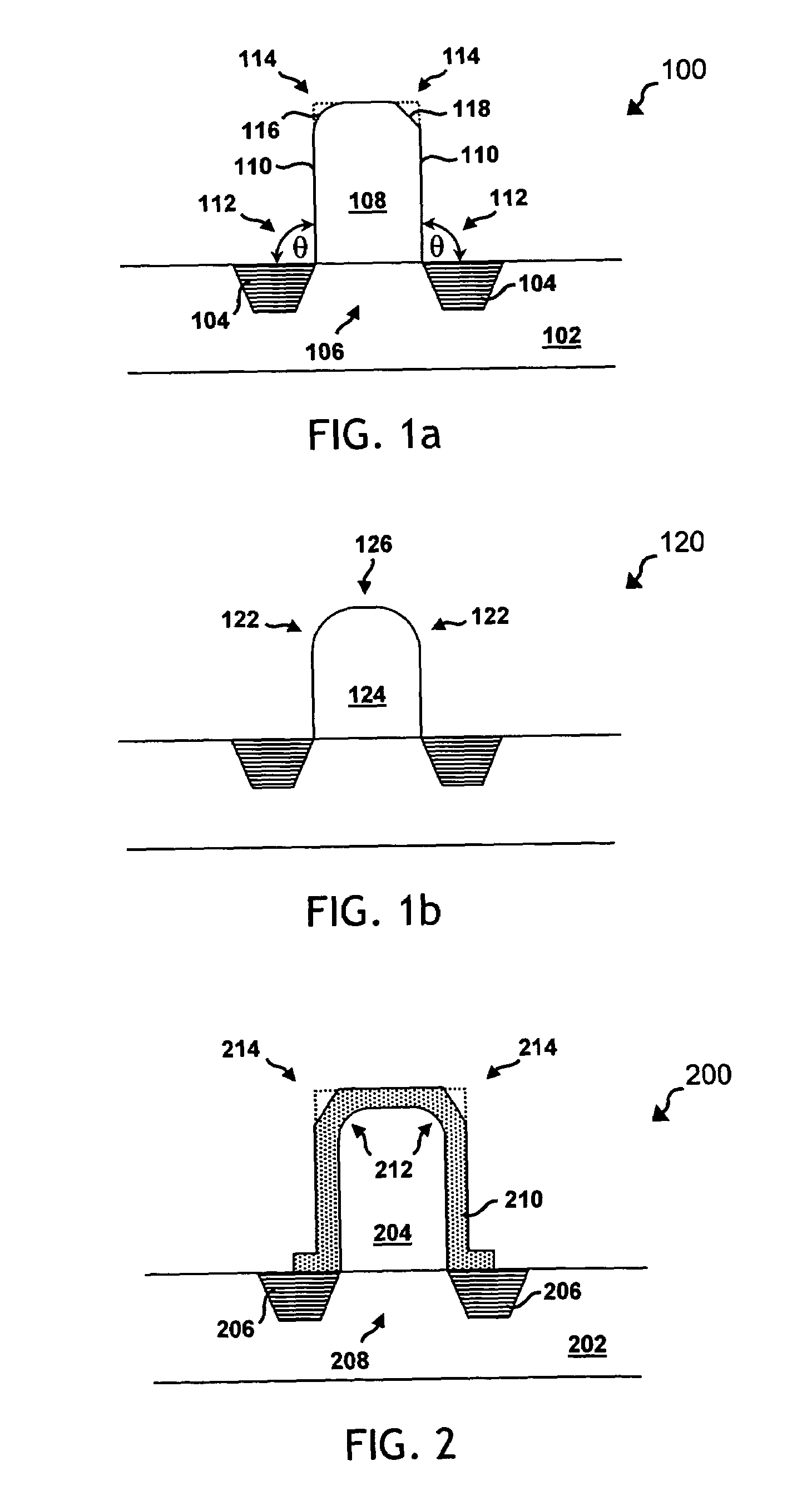
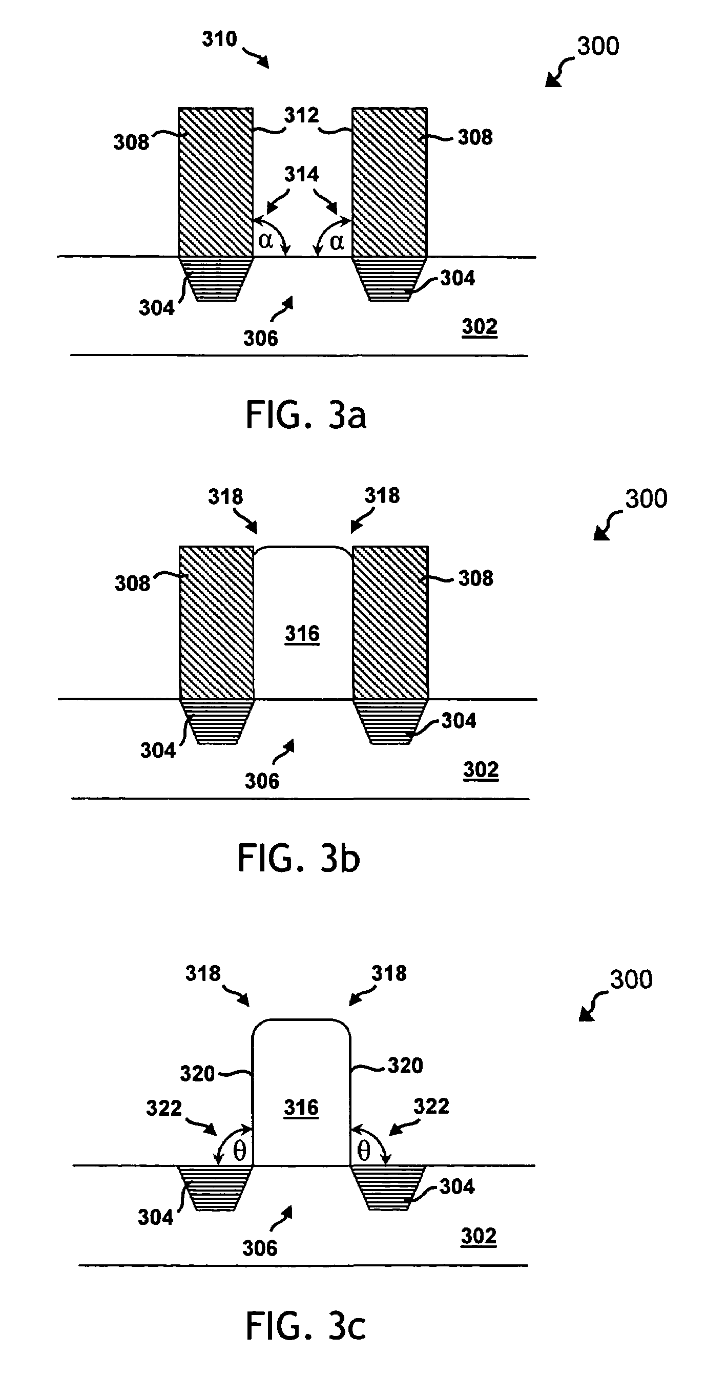
[0023]While the making and using of various embodiments of the present invention are discussed in detail below, it should be appreciated that the present invention provides many applicable inventive concepts, which can be embodied in a wide variety of specific contexts. The present invention is hereafter illustratively described in conjunction with the formation of a triple-gate CMOS transistor. The specific embodiments discussed herein are, however, merely demonstrative of specific ways to make and use the invention and do not limit the scope of the invention.

[0024]Comprehending certain structural, performance and reliability issues inherent in conventional multiple-gate transistor formation, the present invention recognizes that it may be desirable to tailor certain device structures—particularly silicon body structures, utilized as channels—in a selective manner. The present invention further recognizes that it may be desirable to blunt or otherwise nullify square corners or edge...


PUM


Abstract

The present invention provides a system for producing a triple-gate transistor segment (300), utilizing a standard semiconductor substrate (302). The substrate has a plurality of isolation regions (304) formed along its upper surface in a distally separate relationship, defining a channel region (306). A form structure (308) is disposed atop the isolation regions, and defines a channel body area (310) over the channel region. A channel body structure (316) is disposed within the channel body area, and is engineered to provide a blunted corner or edge (318) along a perimeter of its upper exposed surface. The form structure is then removed, and subsequent processing is performed.

Description

RELATED APPLICATIONS[0001]This application is related to U.S. patent application Ser. No. 10 / 696,130, filed on Oct. 29, 2003, entitled MULTIPLE-GATE MOSFET DEVICE WITH LITHOGRAPHY INDEPENDENT SILICON BODY THICKNESS AND METHODS FOR FABRICATING THE SAME, and to U.S. patent application Ser. No. 10 / 696,539, filed on Oct. 29, 2003, entitled TRIPLE GATE MOSFET TRANSISTOR AND METHODS FOR FABRICATING THE SAME, U.S. Pat. No. 6,927,106.TECHNICAL FIELD OF THE INVENTION[0002]The present invention relates generally to the field of semiconductor devices and, more particularly, to apparatus and methods for the production of triple-gated transistors.BACKGROUND OF THE INVENTION[0003]The continual demand for enhanced integrated circuit performance has resulted in, among other things, a dramatic reduction of semiconductor device geometries, and continual efforts to optimize the performance of every substructure within any semiconductor device. A number of improvements and innovations in fabrication pr...

Claims


Application Information

Patent Timeline
Patent Type & Authority Patents(United States)
IPC IPC(8): H01L21/336H01L29/78
CPCH01L29/66484H01L29/7831
Inventor VISOKAY, MARK R.CHAMBERS, JAMES J.
Owner TEXAS INSTR INC
Why Eureka
Try Eureka