Trimming pattern

Inactive Publication Date: 2005-11-29
LAPIS SEMICON CO LTD
View PDF3 Cites 1 Cited by
  • Summary
  • Abstract
  • Description
  • Claims
  • Application Information

AI Technical Summary

Benefits of technology

[0011]It is therefore an object of the invention to provide a novel and improved trimming pattern enabling trimming to be implemented with ease and time required for trimming to be shortened without causing damage to internal elements. The invention provides the trimming pattern for use in trimming of a semiconductor integrated circuit, comprising two pads to which a voltage is applied, a thin line part interconnecting the two pads, and two connecting parts disposed away from each side of the thin line part, and connec

Problems solved by technology

In the case of depositing metal over the level difference, the greater the level difference, the more insufficient coverage of the work surfaces with the metal becomes (the metal layers in stepped parts become thinner in thickness), so that the more miniaturized the metal pattern is, the higher there becomes the probability of a break occurring to the metal pattern, thus creating a cause for deterioration of reliability.
Such planarization has become essential to the process of manufacturing a semiconductor integrated circuit, but has come to cause inco

Method used


Image

  • Trimming pattern
  • Trimming pattern
  • Trimming pattern

Examples


Embodiment Construction

[0016]A preferred embodiment of a trimming pattern according to the invention is described in detail hereinafter with reference to the accompanying drawings. In the present specification and the accompanying drawings, constituent elements of the trimming pattern, having effectively identical functions, are denoted by the same reference numerals, thereby omitting duplicated description.

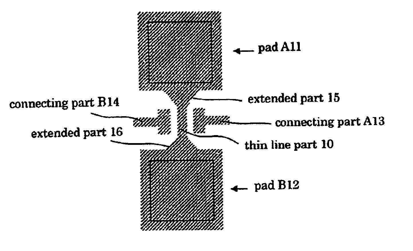
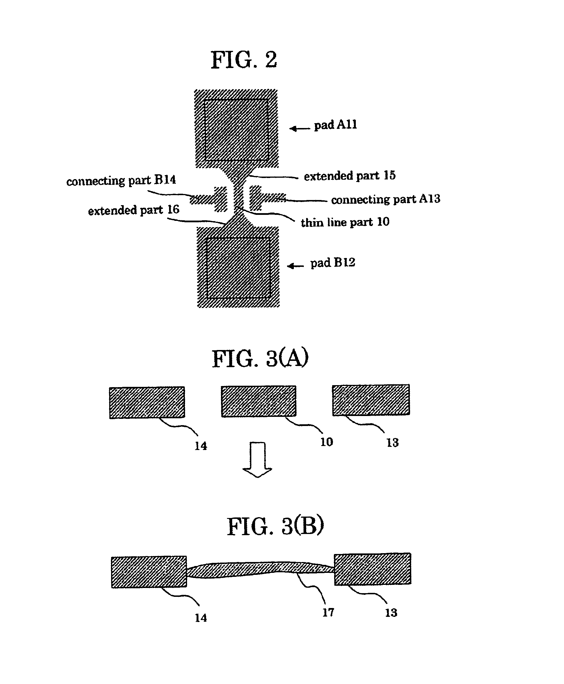
[0017]FIG. 2 is a schematic plan view showing the embodiment of the trimming pattern according to the invention. As with the conventional trimming pattern, there are disposed pads, A11, B12, at respective ends of a thin line part 10 via extended parts, 15, 16, respectively. Connecting parts A13, B14 are formed on each side of the thin line part 10. One end of the connecting parts A13, B14, respectively, opposite from the other end thereof, facing the thin line part 10, is connected to an adjustment circuit, for example, resistors and capacitors, via wiring, and further to a semiconductor integrated cir...


PUM


Abstract

There is provided a trimming pattern enabling trimming to be implemented with ease and time required for trimming to be shortened without causing damage to internal elements. The invention provides the trimming pattern for use in trimming of a semiconductor integrated circuit, comprising two pads to which a voltage is applied, a thin line part interconnecting the two pads, and two connecting parts disposed away from each side of the thin line part, and connected to an adjustment circuit and the semiconductor integrated circuit, respectively. With the invention, trimming is executed by a method of turning the adjustment circuit connected to the connecting parts into the ON state by connecting fused metal of the thin line part to the connecting parts. In this case, since the fused metal can be caused to come into contact with the connecting parts nearby with greater ease than fusion cutting of the thin line part, trimming can be implemented with ease and in shorter time.

Description

FIELD OF THE INVENTION[0001]The present invention relates to a trimming pattern for use in making an adjustment to a semiconductor integrated circuit by selecting ON / OFF for connection with an adjustment circuit prepared in the semiconductor integrated circuit beforehand.BACKGROUND OF THE INVENTION[0002]Trimming is employed in the case of finely adjusting the characteristics of a semiconductor integrated circuit in whole, in particular, an analog circuit, by changing its resistance value, capacitance value, and inductance, aside from the inherent characteristics of a semiconductor device. Common methods of trimming include a laser trimming method, and a method of trimming by causing current to flow to pads connected to resistors and capacitors and by cutting wiring.[0003]Herein, the laser trimming method is a method for executing trimming by directly burning off or cutting down resistance elements, and is capable of fine adjustment, but requires a dedicated apparatus using a laser. ...

Claims


Application Information

Patent Timeline
IPC IPC(8): H01L21/82H01L27/04H01L21/822H01L23/525
CPCG11C29/028H01L23/5252H01L2924/0002H01L2924/00
Inventor TSUJII, YASUHARUMORIMOTO, HARUAKIOKUI, YUTAKA
Owner LAPIS SEMICON CO LTD
Why Eureka
Try Eureka