Low stress semiconductor device coating and method of forming thereof

Active Publication Date: 2006-06-08
TAIWAN SEMICON MFG CO LTD
View PDF7 Cites 0 Cited by
  • Summary
  • Abstract
  • Description
  • Claims
  • Application Information

AI Technical Summary

Benefits of technology

[0010] Advantages of an embodiment of the present invention are the ease of implementation and low cost. Polyimides have been used for years in the semiconductor industry in the manufacture of printed circuit boards, as an interdielectric layer between conductors, and as a wafer planariza

Problems solved by technology

Localized fracture of the dielectric film near a conducting line may lead to catastrophic failure of the chip.
Generally, one cause of fracture is stress arising from a mismatch in coefficients of thermal expansion combined with weak interfacial adhesion.
These problems generally are compounded when low dielectric constant (low-k) materials are used in the device.
Because the mechanical strength of low-k materials is typically less than that of oxides and glasses, stress between the polyimide layer and the underlying low-k layer or layers ma

Method used


Image

  • Low stress semiconductor device coating and method of forming thereof
  • Low stress semiconductor device coating and method of forming thereof
  • Low stress semiconductor device coating and method of forming thereof

Examples


Embodiment Construction

[0016] The making and using of the presently preferred embodiments are discussed in detail below. It should be appreciated, however, that the present invention provides many applicable inventive concepts that can be embodied in a wide variety of specific contexts. The specific embodiments discussed are merely illustrative of specific ways to make and use the invention, and do not limit the scope of the invention.

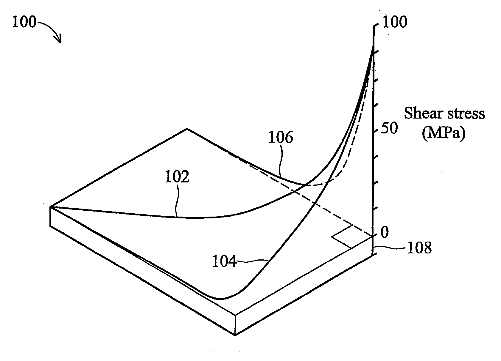
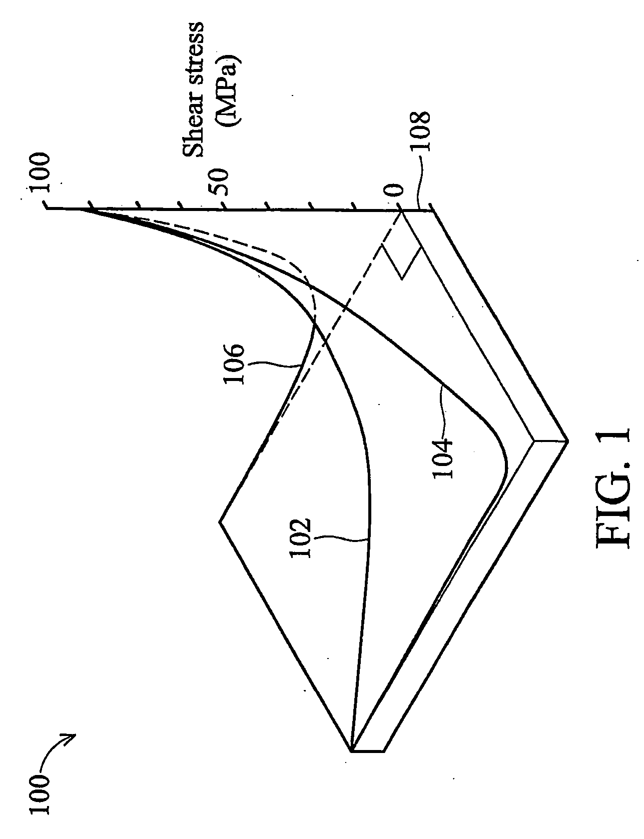
[0017] The present invention will be described with respect to preferred embodiments in a specific context, namely a semiconductor device having a polyimide overcoat overlying a low-k layer, except for a selected region. The invention also applies, for example, to other coating applications in which corner stress or corner delamination may be a problem, for example polymeric materials, such as benzocyclobutene (BCB).

[0018] Embodiments of the present invention may be particularly useful with dies comprising low-k materials. An exemplary low-k inorganic material that is freq...


PUM


Abstract

A low stress, protective coating for a semiconductor device and a method for its manufacture. A preferred embodiment comprises coating the top surface of a semiconductor die with polyimide except for corner regions of the die. Not having corners in the polyimide protective overcoat generally reduces shear stresses in the die. Reducing stress, in turn, generally reduces the occurrence of problems such as fracture, delamination, or cracking within the die. A low stress coating may be particularly advantageous in semiconductor devices having low-k insulating materials, which are generally of low mechanical strength.

Description

TECHNICAL FIELD [0001] The present invention relates generally to semiconductor devices and manufacturing methods and more particularly to a semiconductor device having a low stress coating and a method of forming thereof. BACKGROUND [0002] Polyimide films are frequently used as a protective overcoat for semiconductor devices. Manufacturers commonly apply a polyimide layer to the top of a semiconductor device. This may be done before grinding, dicing, and final packaging of the semiconductor device. The protective overcoat may function as a stress buffer and as an attenuation layer for soft error rate (SER) reduction. The protective overcoat generally protects the delicate device components from damage during handling and moisture penetration. [0003] In a semiconductor device, it is preferable for adjacent layers to have good adhesion to one other. For example, when coating a material such as a copper metallization, adhesion between the dielectric and the copper may be a reliability...

Claims


Application Information

Patent Timeline
IPC IPC(8): H01L21/4763
CPCH01L23/3171H01L2924/0002H01L2924/00
Inventor JENG, SHIN-PUU
Owner TAIWAN SEMICON MFG CO LTD
Why Eureka
Try Eureka