Heating configuration for use in thermal processing chambers

a technology for thermal processing chambers and heating configurations, which is applied in the direction of crystal growth processes, drying machines, baking ovens, etc., can solve the problems of limiting the ability, limiting the ability to perform various other chemical and physical processes on the wafers, and affecting the performance of the wafer, so as to minimize the problem of reflectivity

Inactive Publication Date: 2005-11-29
MATTSON TECHNOLOGY +1
View PDF145 Cites 48 Cited by
  • Summary
  • Abstract
  • Description
  • Claims
  • Application Information

AI Technical Summary

Benefits of technology

[0010]During the heating process, the semiconductor wafer can be rotated. In this manner, the light energy sources form radial heating zones on the wafer which aid in heating the wafer uniformly and provide good temporal control during the heating cycle.
[0012]The tuning devices proved localized temperature control on the wafer. Through the combination of linear lamps and tuning sources, the present invention allows the processing system to achieve a better temperature uniformity across the wafer or a better realization of a desired temperature profile. In one embodiment, the system can also be used to radially fine tune the whole wafer for further improving temperature uniformity.
[0014]Further, since most lasers emit light at a particular wavelength, in an alternative embodiment of the present invention, multiple lasers can be used that emit light at different wavelengths. By using different types of lasers, problems associated with reflectivity can be minimized.

Problems solved by technology

Problems have been experienced in the past, however, in being able to maintain a constant temperature throughout the wafer and in being able to control the rate at which the wafer is heated.
If the wafer is heated nonuniformly, various unwanted stresses can develop in the wafer.
Not being able to heat the wafers uniformly also limits the ability to uniformly deposit films on the wafers, to uniformly etch the wafers, beside limiting the ability to perform various other chemical and physical processes on the wafers.
These systems, however, have become increasingly complex and expensive to produce.

Method used


Image

  • Heating configuration for use in thermal processing chambers
  • Heating configuration for use in thermal processing chambers
  • Heating configuration for use in thermal processing chambers

Examples


Embodiment Construction

[0028]It is to be understood by one of ordinary skill in the art that the present discussion is a description of exemplary embodiments only, and is not intended as limiting the broader aspects of the present invention, which broader aspects are embodied in the exemplary construction.

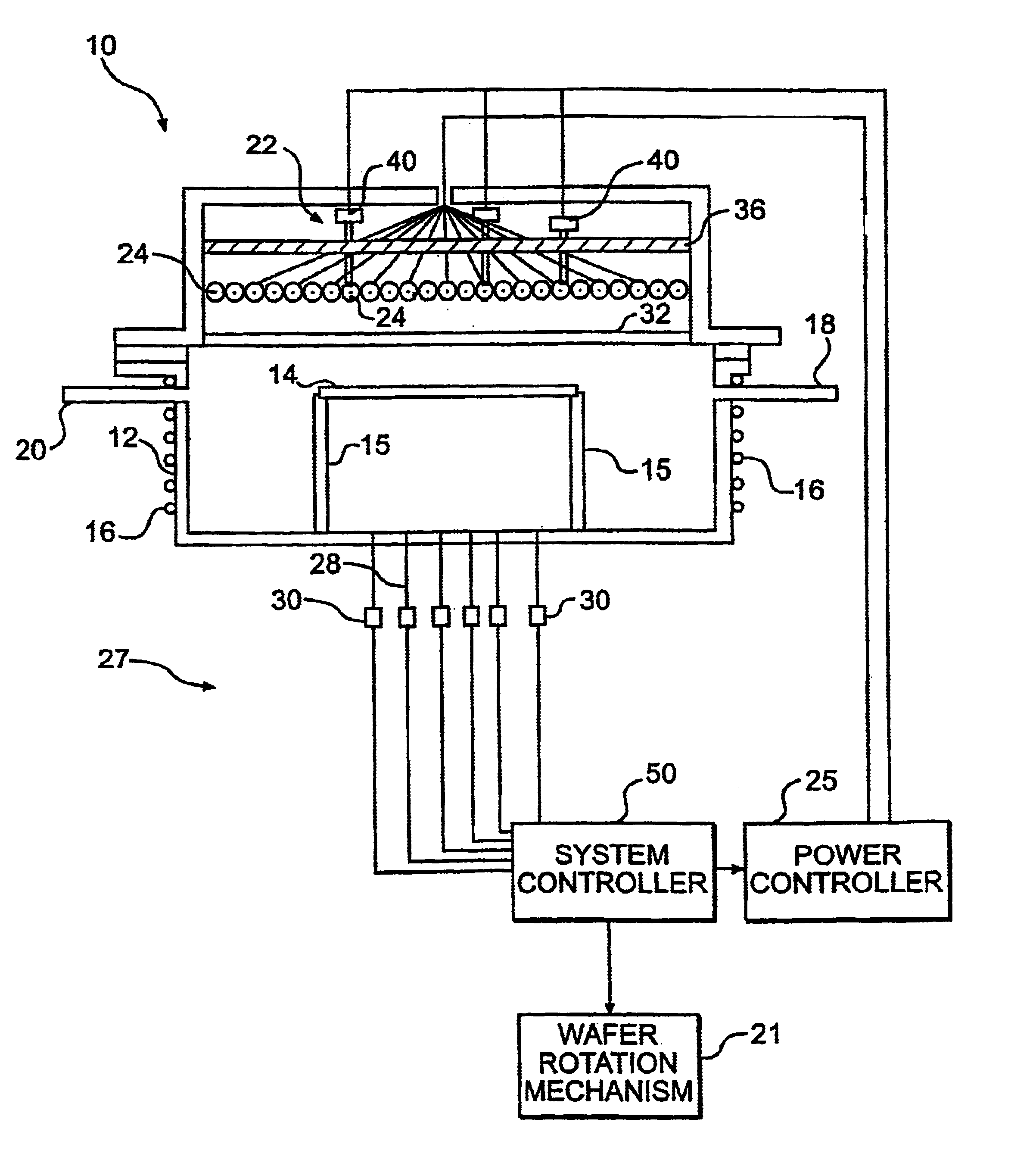
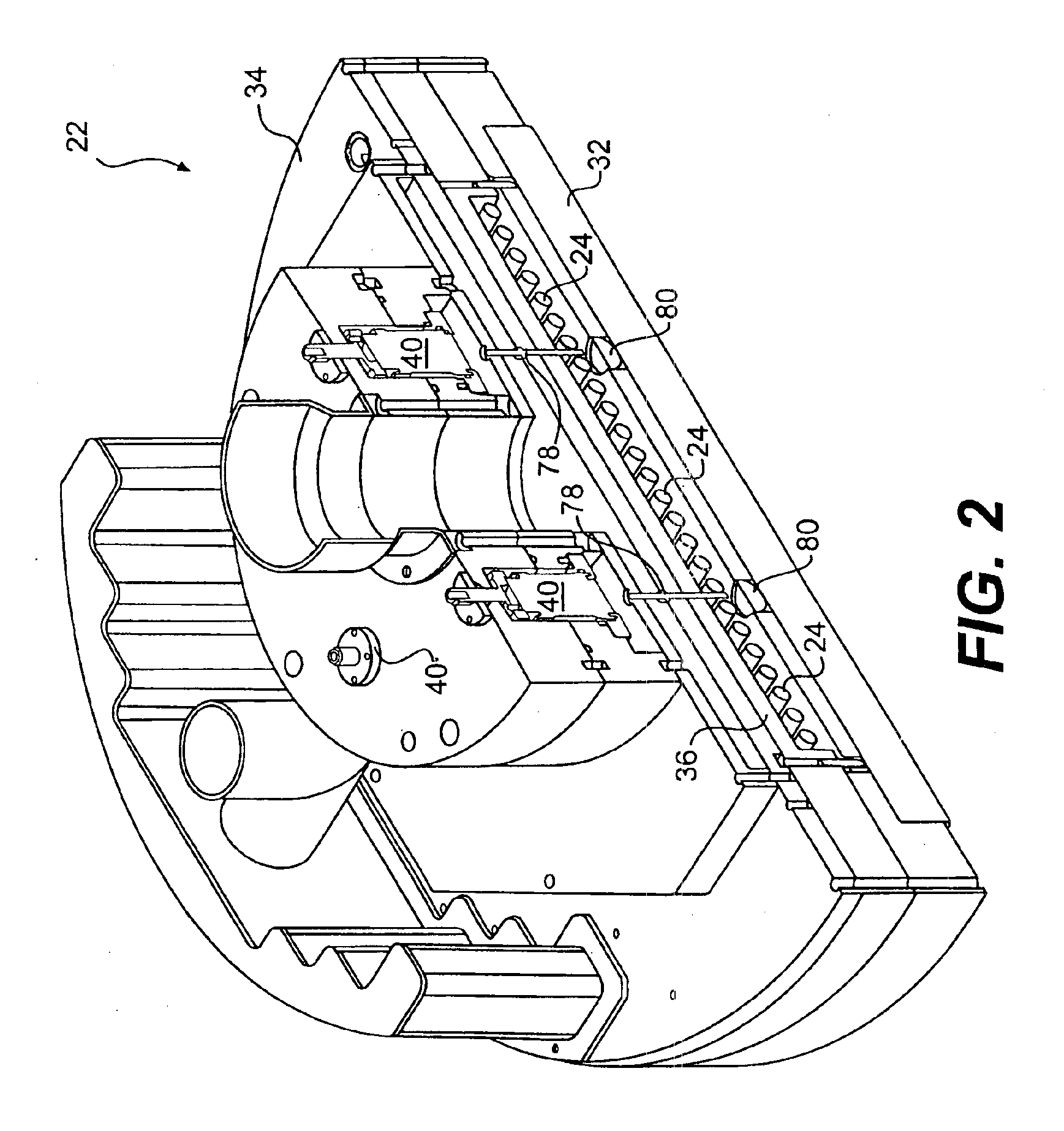
[0029]A rapid thermal processing apparatus uses intense light to heat a semiconductor wafer as part of the manufacturing process of integrated circuits. Exposure to light energy causes a rapid increase in the temperature of a semiconductor wafer and allows processing times to be relatively short. In rapid thermal processing systems, it is important to radiate the wafer with very high intensity light in a very uniform and controlled fashion. As stated above, the difficulty with current devices is that the requirements for the intensity of the radiated light and the ability to heat wafers uniformly are very difficult to achieve.

[0030]In general, the present invention is directed to an apparatus and method ...


PUM

PropertyMeasurementUnit
angle of incidenceaaaaaaaaaa
temperaturesaaaaaaaaaa
angle of incidenceaaaaaaaaaa

Abstract

An apparatus for heat treating semiconductor wafers is disclosed. The apparatus includes a heating device which contains an assembly linear lamps for emitting light energy onto a wafer. The linear lamps can be placed in various configurations. In accordance with the present invention, tuning devices which are used to adjust the overall irradiance distribution of the light energy sources are included in the heating device. The tuning devices can be, for instance, are lamps or lasers.

Description

BACKGROUND OF THE INVENTION[0001]A thermal processing chamber as used herein refers to a device that rapidly heats objects, such as semiconductor wafers. Such devices typically include a substrate holder for holding a semiconductor wafer and a light source that emits light energy for heating the wafer. During heat treatment, the semiconductor wafers are heated under controlled conditions according to a preset temperature regime. For monitoring the temperature of the semiconductor wafer during heat treatment, thermal processing chambers also typically include temperature sensing devices, such as pyrometers, that sense the radiation being emitted by the semiconductor wafer at a selected band of wavelengths. By sensing the thermal radiation being emitted by the wafer, the temperature of the wafer can be calculated with reasonable accuracy.[0002]In alternative embodiments, instead of or in addition to using radiation sensing devices, thermal processing chambers can also contain thermoco...

Claims


Application Information

Patent Timeline
Patent Type & Authority Patents(United States)
IPC IPC(8): C23C16/48C30B25/10C30B31/12H01L21/00
CPCC23C16/481C30B25/105C30B31/12H01L21/67115
Inventor KOREN, ZIONO'CARROLL, CONOR PATRICKCHOY, SHUEN CHUNTIMANS, PAUL JANISCARDEMA, RUDY SANTO TOMASTAOKA, JAMES TSUNEOSTROD, ARIEH A.
Owner MATTSON TECHNOLOGY
Why Eureka
Try Eureka