Method of forming an element of a microelectronic circuit

Inactive Publication Date: 2005-12-06
INTEL CORP
View PDF9 Cites 34 Cited by
  • Summary
  • Abstract
  • Description
  • Claims
  • Application Information

AI Technical Summary

Problems solved by technology

Semiconductor fabrication environments, however, rarely make provision for attachment of wafers to one another and

Method used


Image

  • Method of forming an element of a microelectronic circuit
  • Method of forming an element of a microelectronic circuit
  • Method of forming an element of a microelectronic circuit

Examples


Embodiment Construction

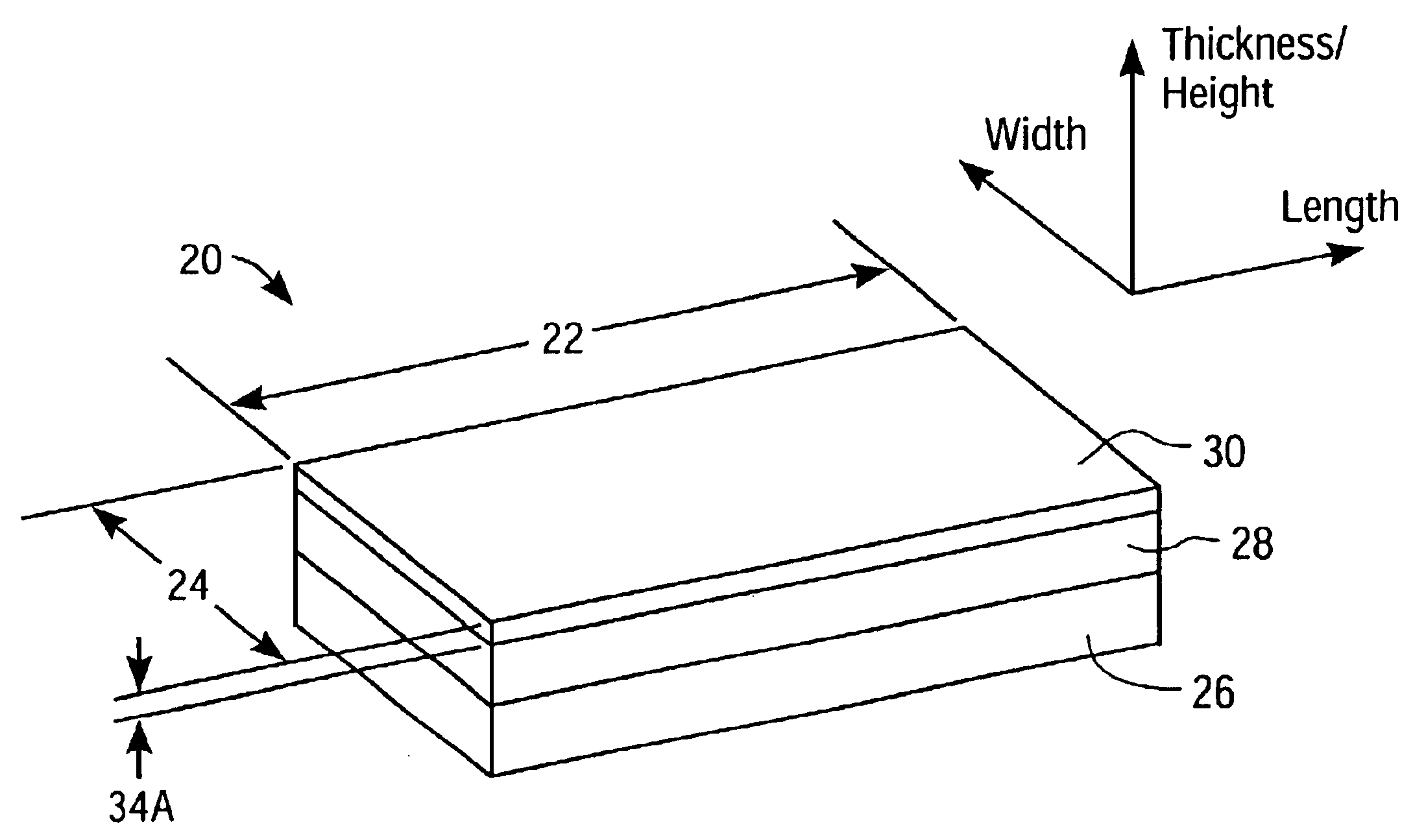
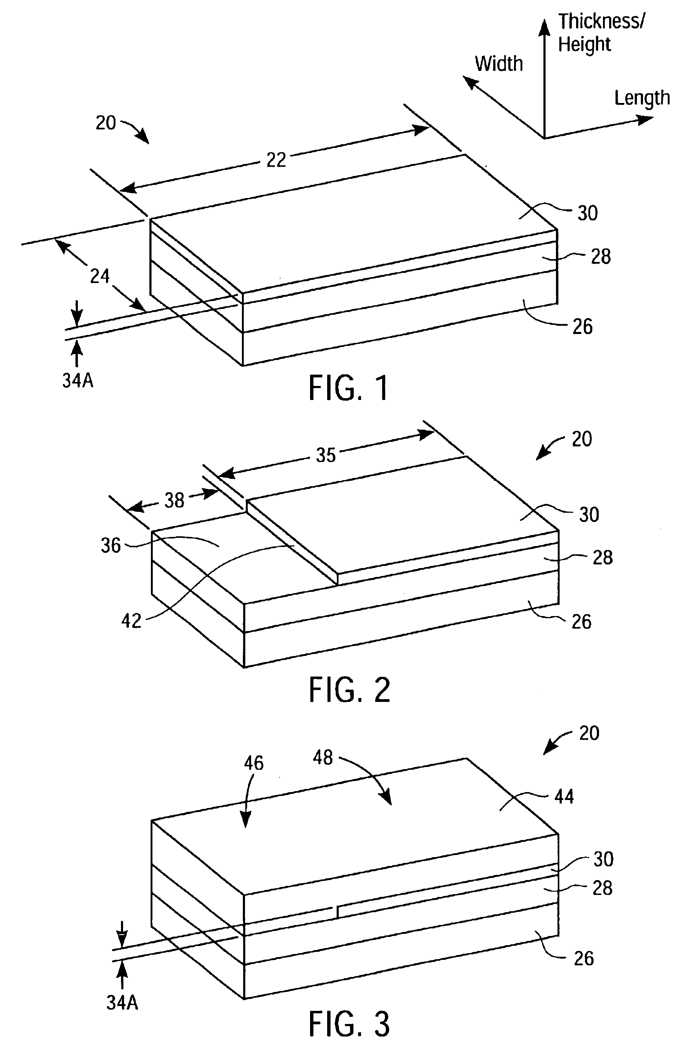
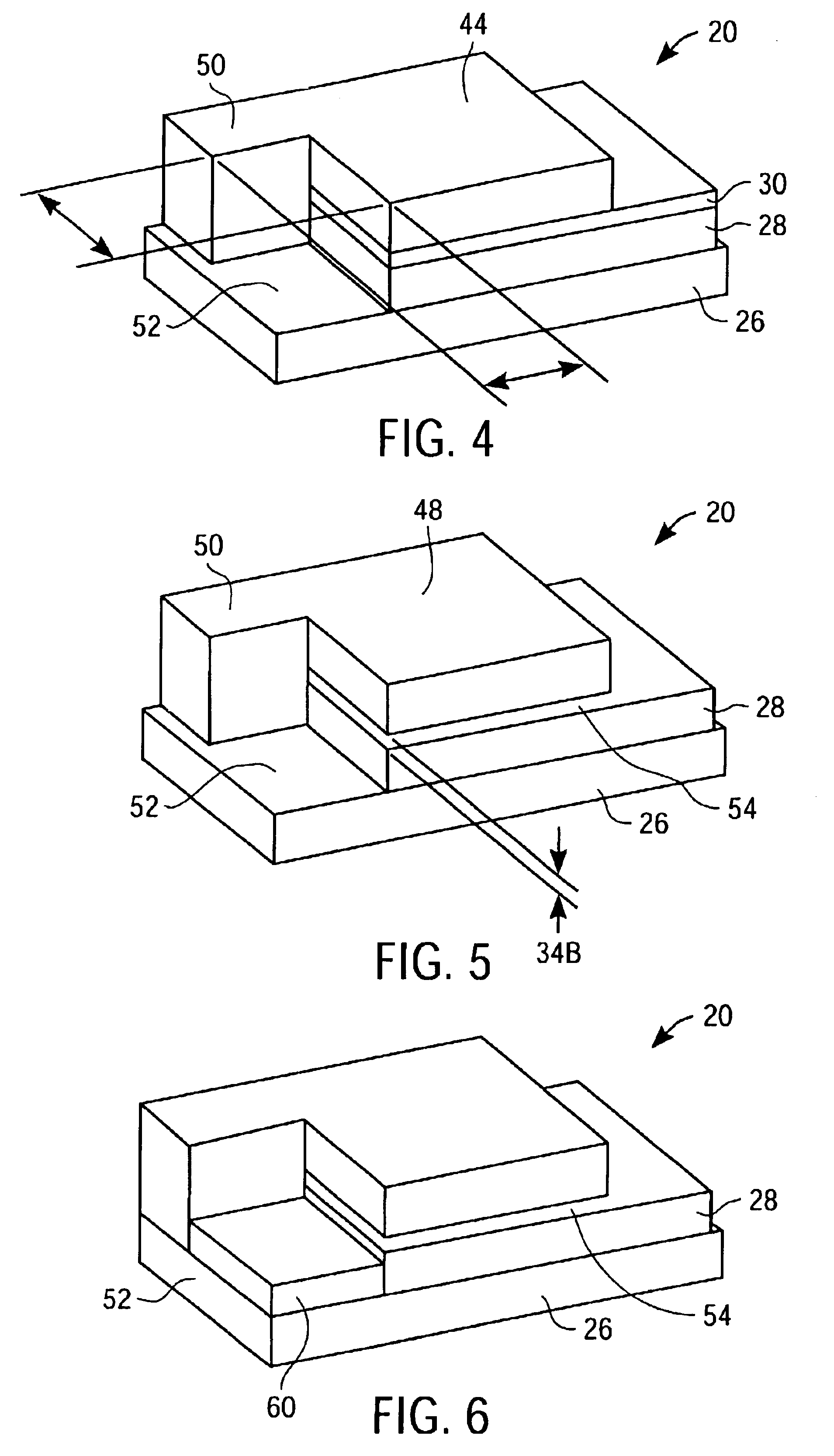
[0022]In the following description, terms such as horizontal, vertical, width, length, height, and thickness are used. These terms are used to describe and define orientations of structures and surfaces relative to one another, and should not be interpreted as pertaining to an absolute frame of reference.

[0023]FIG. 1 of the accompanying drawings illustrates a portion 20 out of a partially fabricated wafer, having a width 22 and a length 24. The portion 20 includes a conventional silicon monocrystalline substrate 26, a supporting silicon dioxide (SiO2) dielectric layer 28 formed on the monocrystalline substrate 26, and a silicon nitride (Si2NO3) sacrificial layer 30 formed on the dielectric layer 28. The substrate may, for example, be silicon (Si), germanium (Ge), silicon germanium (SixGey), gallium arsenide (GaAs), InSb, GaP, GaSb, or carbon. The sacrificial layer 30 has a thickness 34A which is extremely thin, typically on the order of a few nanometers. A process for forming 15 nm ...


PUM


Abstract

A method is described for forming an element of a microelectronic circuit. A sacrificial layer is formed on an upper surface of a support layer. The sacrificial layer is extremely thin and uniform. A height-defining layer is then formed on the sacrificial layer, whereafter the sacrificial layer is etched away so that a well-defined gap is left between an upper surface of the support layer and a lower surface of the height-defining layer. A monocrystalline semiconductor material is then selectively grown from a nucleation silicon site through the gap. The monocrystalline semiconductor material forms a monocrystalline layer having a thickness corresponding to the thickness of the original sacrificial layer.

Description

BACKGROUND OF THE INVENTION[0001]1). Field of the Invention[0002]This invention relates to a method of forming an element of a microelectronic circuit and to a device that includes the element.[0003]2). Discussion of Related Art[0004]Nanotechnology involves the formation of extremely small structures with dimensions on the order of nanometers in multiple directions.[0005]Certain devices, for example, silicon on insulator (SOI) devices, require that a monocrystalline silicon or other monocrystalline semiconductor material be formed on an insulating dielectric layer. Various techniques exist that can be used for creating a monocrystalline semiconductor layer on an insulating layer. Such techniques usually involve the implantation of ions to a specific depth into a monocrystalline semiconductor material, attaching a dielectric layer of another wafer to the semiconductor material, subsequently shearing the semiconductor material at a depth to which the ions are implanted, whereafter a t...

Claims


Application Information

Patent Timeline
IPC IPC(8): H01L21/20H01L29/12H01S5/34
CPCB82Y10/00B82Y20/00H01L29/125H01L29/66795H01L21/0262H01L21/02381H01L21/02387H01L21/02532H01L21/02538H01S5/341
Inventor DOYLE, BRIAN S.MURTHY, ANAND S.CHAU, ROBERT S.
Owner INTEL CORP
Why Eureka
Try Eureka