Method of reducing process plasma damage using optical spectroscopy

a technology of optical emission spectroscopy and plasma damage reduction, which is applied in the direction of semiconductor/solid-state device testing/measurement, instruments, material analysis, etc., can solve the problems of high leakage, weak gate oxide, and charge accumulated on the poly gate, so as to avoid plasma processing damage

Inactive Publication Date: 2005-12-06
BELL SEMICON LLC
View PDF3 Cites 76 Cited by
  • Summary
  • Abstract
  • Description
  • Claims
  • Application Information

AI Technical Summary

Benefits of technology

[0011]To achieve the foregoing, the present invention provides methods and apparatus for determining plasma charge voltages and correlating plasma damage using optical emission spectra. The present invention provides an improved process for determining species contributing to plasma charging damage and using optical emission spectra for those species to optimize the plasma process or to control the plasma process. The present invention also provides an apparatus t

Problems solved by technology

If the plasma charge voltage is high, such as, for example, exceeding 6 volts, the charge accumulated on the poly gates can damage the gate oxide.
This results in a weak gate oxide and induces high leakage.
But testing using WLR wafers to identify plasma charging damage is exceeding slow, sometimes taking several weeks or months to receive the data feedback.
Finally, results from individual plasma process steps interact wi

Method used


Image

  • Method of reducing process plasma damage using optical spectroscopy
  • Method of reducing process plasma damage using optical spectroscopy
  • Method of reducing process plasma damage using optical spectroscopy

Examples


Embodiment Construction

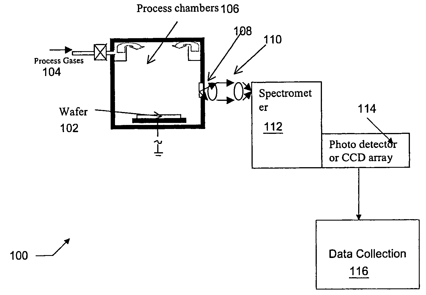
[0020]Reference will now be made in detail to preferred embodiments of the invention. Examples of the preferred embodiments are illustrated in the accompanying drawings. While the invention will be described in conjunction with these preferred embodiments, it will be understood that it is not intended to limit the invention to such preferred embodiments. On the contrary, it is intended to cover alternatives, modifications, and equivalents as may be included within the spirit and scope of the invention as defined by the appended claims. In the following description, numerous specific details are set forth in order to provide a thorough understanding of the present invention. The present invention may be practiced without some or all of these specific details. In other instances, well known process operations have not been described in detail in order not to unnecessarily obscure the present invention.

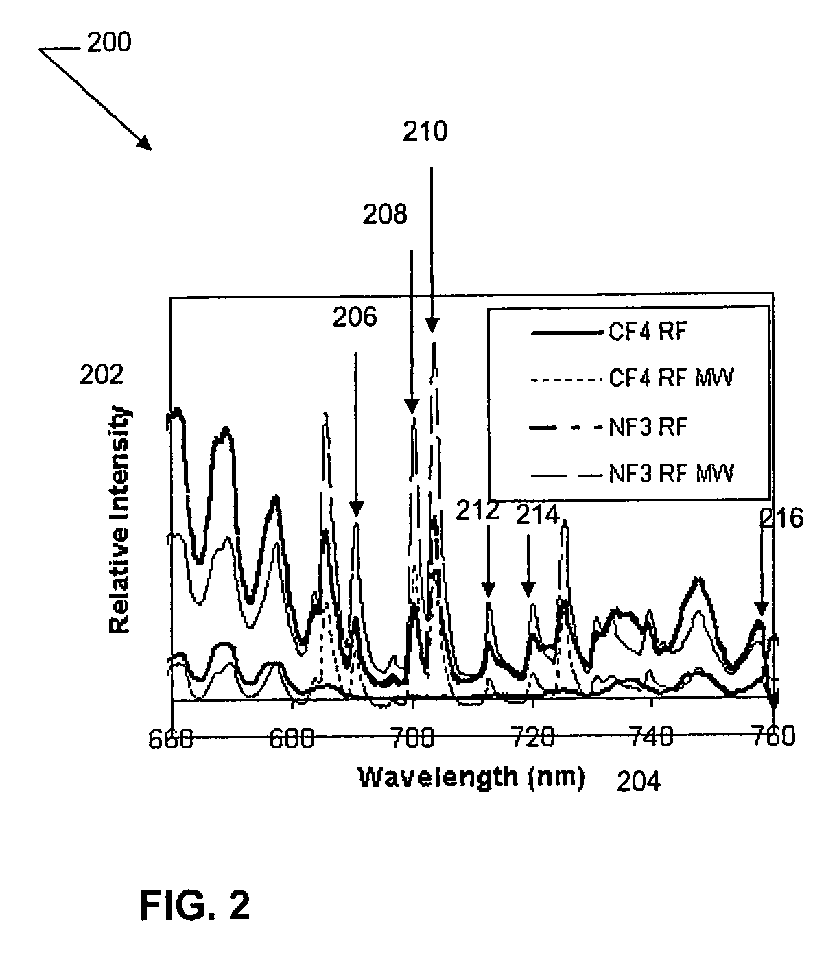
[0021]The present invention provides in one embodiment an improved process for deter...


PUM


Abstract

Optical emission spectra from a test wafer during a plasma process are measured using a spectrometer. The plasma charging voltage retained by (detected by) the test wafer is measured after the process step is completed. The emission spectra are correlated with the plasma charging voltage to identify the species contributing to the plasma charging voltage. The optical emission spectra are monitored in real time to optimize the plasma process to prevent plasma charging damage. The optical emission spectra are also monitored to control the plasma process drift.

Description

CROSS-REFERENCE TO RELATED APPLICATION[0001]This is a Divisional application of prior application Ser. No. 10 / 195,775 filed on Jul. 12, 2002, now U.S. Pat. No. 6,673,200.[0002]This application takes priority under U.S.C. 119(e) of U.S. Provisional Application No. 60 / 384,499 filed May 30, 2002 entitled, “METHOD OF REDUCING PROCESS PLASMA DAMAGE USING OPTICAL SPECTROSCOPY” by Shiqun Gu, Peter McGrath, and Ryan Fujimoto, which is incorporated by reference in its entirety for all purposes.BACKGROUND OF THE INVENTION[0003]1. Field of the Invention[0004]The present invention relates to processes for monitoring plasma charging in semiconductor wafers. More particularly, the present invention relates to the use of optical emission spectroscopy in plasma etching and deposition processes.[0005]2. Description of the Related Art[0006]Semiconductor wafer fabrication involves a series of processes used to create semiconductor devices and integrated circuits (ICs) in and on a semiconductor wafer s...

Claims


Application Information

Patent Timeline
IPC IPC(8): H01J37/32H01L21/00H01L23/544
CPCH01J37/32935H01J37/32972H01L22/34Y10T156/1734H01L21/67253H01L21/67069
Inventor GU, SHIQUNMCGRATH, PETER GERARDFUJIMOTO, RYAN TADASHI
Owner BELL SEMICON LLC
Why Eureka
Try Eureka