Self-aligned mask to reduce cell layout area

a cell layout and self-aligning technology, applied in the manufacture of semiconductor/solid-state devices, basic electric elements, electric devices, etc., can solve the problems of reducing yield, waste of full wafers of devices, and increasing the area of each via, so as to achieve high capacitance, high density, and high capacitance

Inactive Publication Date: 2005-12-13
IBM CORP +1
View PDF4 Cites 10 Cited by
  • Summary
  • Abstract
  • Description
  • Claims
  • Application Information

AI Technical Summary

Benefits of technology

[0004]These and other problems are generally solved or corrected, and technical advantages are generally achieved, by embodiments of the present invention which provide methods for providing self-aligned features, such as, for example, vias or trenches, on a semiconductor device. The method comprises recessing the top surface of one or more conductors or lines of metallization typically deposited by the Damascene process below the top surface of the surrounding dielectric layer. Recessing the metal may be accomplished by a plasma etch that is selective to the dielectric material or any other suitable process. The recessed conductor or metal lines are then capped by depositing a barrier layer over the top surface of the substrate. The barrier layer may be any suitable material including silicon nitride and silicon carbide and covers the substrate and recessed metal as a substantially constant thickness or conformal coating. Thus, the capping or barrier layer will include a recess directly above the recessed metal lines. According to one embodiment, an intermediate conformal coating or layer of dielectric (ILD) is then deposited over the capping or barrier layer followed by the deposition of a conformal coating of a liner material, such as for example, Tantalum (Ta), Titanium (Ti), Tantalum Nitride (TaN), Titanium Nitride (TiN), Silicon Nitride (SiN) or Silicon Carbide (SiC). However, for certain applications and depending on future processing steps, it may be appropriate to eliminate the depositing of the ILD and deposit the liner material directly over the conformal capping or barrier layer. The layer of liner material is then planarized such that the “high” areas of the conformal liner are removed so that only the low areas remain. However, the “low” areas will also be directly above (aligned with) the metal lines recessed below the top surface of the surrounding dielectric materials. Therefore, by using the remaining areas of the liner layer as a hard mask, vias can be etched through the dielectric layer of the substrate that are very close to, but not in contact with, the adjacent conductor or line of metallization. Similarly, higher density wiring can be obtained by using this method to etch trenches that extend to a relatively shallow depth in the dielectric. For circuit building purposes, it may be advantageous to create structures with very high capacitance, in which case trenches or similar structures may be formed using the methods of this invention, and which serve the purpose of creating circuit elements with high capacitance. It can therefore be seen that, while via formation is an ideal use of this invention's techniques, one is not limited to forming vias only.

Problems solved by technology

Since electrical circuits and devices in an integrated chip are very small, a via that does successfully connect two levels of circuits together, but is misaligned by only a few tenths of microns may cause shorts and render a full wafer of devices useless.
Unfortunately, since each of such multi-layer devices will typically include several vias, and since each wafer includes hundreds of devices, increasing the area for each via is also wasteful and decreases yield.

Method used


Image

  • Self-aligned mask to reduce cell layout area
  • Self-aligned mask to reduce cell layout area
  • Self-aligned mask to reduce cell layout area

Examples


Embodiment Construction

[0009]The making and using of the presently preferred embodiments are discussed in detail below. It should be appreciated, however, that the present invention provides many applicable inventive concepts that can be embodied in a wide variety of specific contexts. The specific embodiments discussed are merely illustrative of specific ways to make and use the invention, and do not limit the scope of the invention.

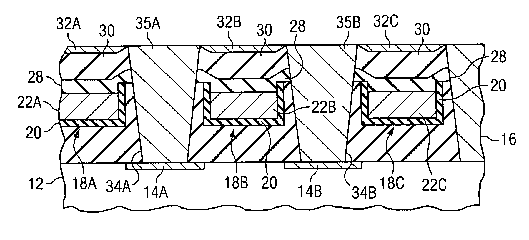
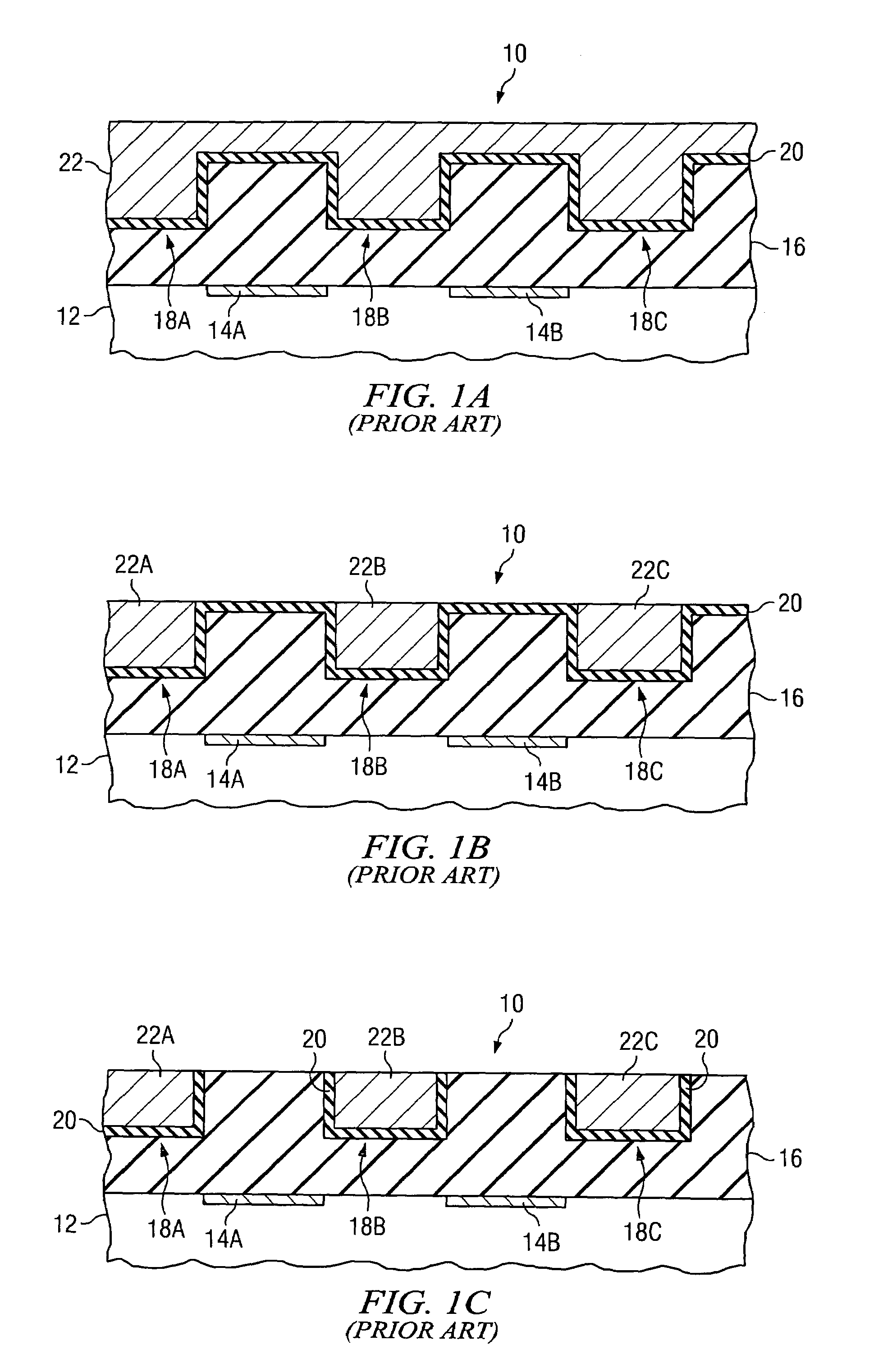
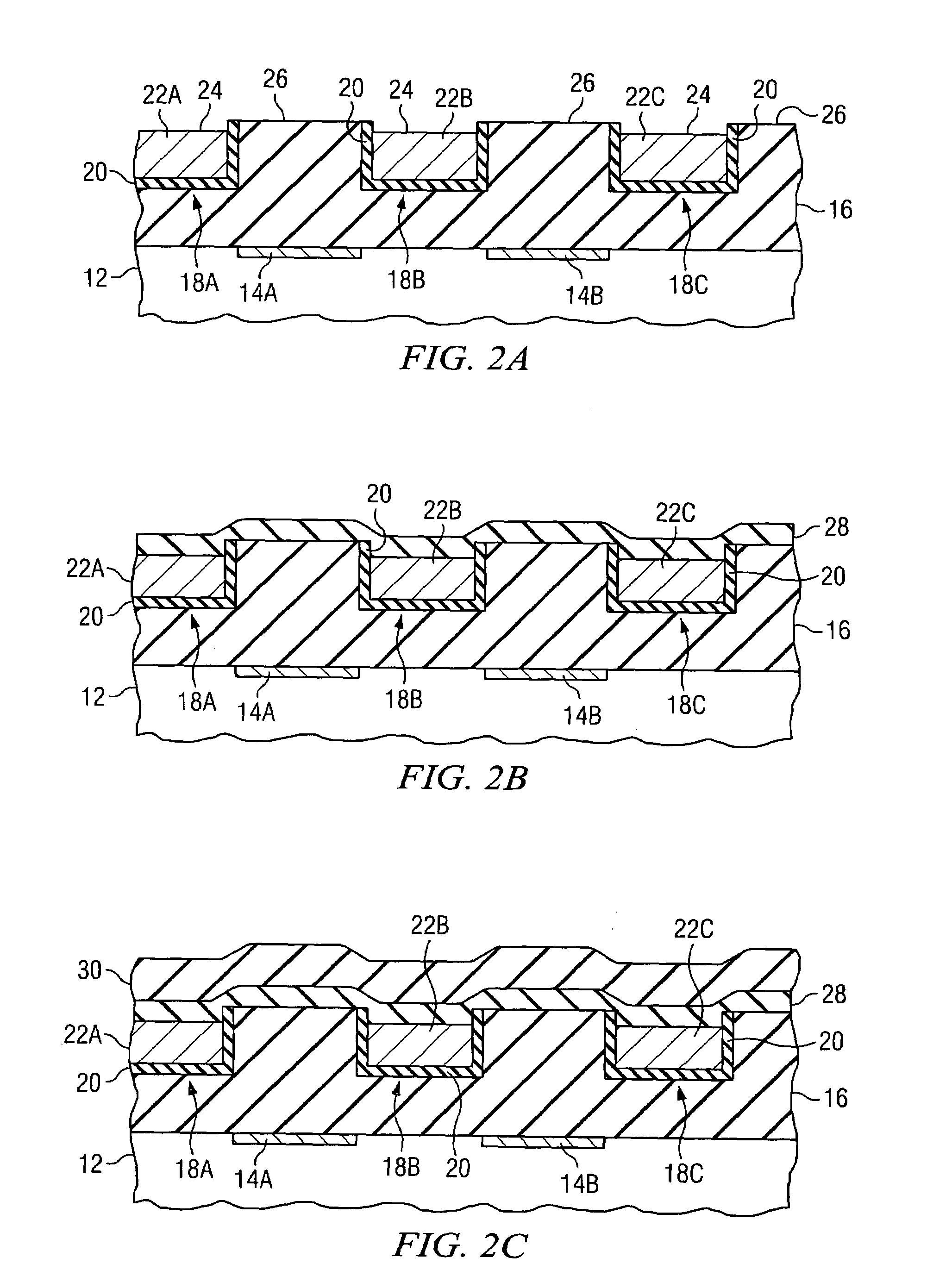
[0010]Referring now to the prior art FIG. 1A, there is shown a cross-section of a substrate with conductor or lines of metallization formed in a dielectric. Typically, the lines of metallization will be formed by the Damascene process but could be formed by any other suitable technique. As shown, a substrate 10 is comprised of a first level of dielectric 12 which may include a multiplicity of various types of selected circuits. For example, the connecting pads 14a and 14b may represent connections to lines of metallization or terminals of various circuits such as the bit line...


PUM


Abstract

Self-aligning vias and trenches etched between adjacent lines of metallization allows the area of the dielectric substrate allocated to the via or trench to be significantly reduced without increasing the possibility of electrical shorts to the adjacent lines of metallization.

Description

TECHNICAL FIELD[0001]The present invention relates to the manufacture of semiconductor devices and more particularly to a method of reducing the area of a semiconductor cell by using a self-aligned mask for etching selected features, such as a via or trench, from an upper level of metallization through an intermediate dielectric to possibly contact lower level circuits or metallization.BACKGROUND[0002]As will be appreciated by those skilled in the art, most semiconductor devices have several layers of circuits interconnected by vias etched through insulating and / or dielectric materials separating the two levels of circuits and filled with a conductive material such copper, gold, silver or aluminum. To avoid electrical shorts, it is very important that these vias filled with conductive metals do not unintentionally come into contact with other conductive lines and / or devices. Since electrical circuits and devices in an integrated chip are very small, a via that does successfully conn...

Claims


Application Information

Patent Timeline
Patent Type & Authority Patents(United States)
IPC IPC(8): H01L21/60
CPCH01L21/76897H01L21/76834
Inventor COSTRINI, GREGORYLOW, KIA-SENGRATH, DAVID L.GAIDIS, MICHAEL C.GLASHAUSER, WALTER
Owner IBM CORP
Why Eureka
Try Eureka