Active matrix type display apparatus, active matrix type organic electroluminescence display apparatus, and driving methods thereof

a display apparatus and active matrix technology, applied in the direction of identification means, instruments, static indicating devices, etc., can solve the problems of crystallinity and inferior controllability of the conducting mechanism to single-crystal silicon, the difficulty in realizing a large high-definition display, and the passive matrix method, so as to reduce the transistor size of the tft provided in the pixel circuit and reduce the writing time

Inactive Publication Date: 2005-12-13
SONY CORP
View PDF8 Cites 31 Cited by
  • Summary
  • Abstract
  • Description
  • Claims
  • Application Information

AI Technical Summary

Benefits of technology

[0026]It is an object of the present invention to provide an active matrix type display apparatus, an active matrix type organic EL display apparatus, and driving methods thereof that make it possible to increase the display size and resolution by reducing the data writing time while preventing an increase in size of transistors in a pixel circuit when a current writing type pixel circuit is used.
[0028]The current control means, which is a characteristic part of the present invention, handles the bypass current of the data line current. It is thereby possible to substantially reduce time for writing the data current flowing through TFTs provided in the pixel circuit. In addition, when the writing time is set unchanged, transistor size of the TFTs provided in the pixel circuit can be reduced. An organic EL device having a first electrode, a second electrode, and an organic layer including a light emitting layer between the first electrode and the second electrode, for example, is used as the electrooptic device in the present invention.

Problems solved by technology

While the passive matrix method has a simple construction, the passive matrix method has problems such as difficulty in realizing a large high-definition display.
Controlling variations in characteristics of the thin film transistor and compensating for variations in the characteristics of the thin film transistor by circuit means are major problems of the active matrix type organic EL display using the thin film transistor in the pixel circuit.
In fact, it is known that amorphous silicon and polysilicon used to form the TFT have inferior crystallinity and inferior controllability of the conducting mechanism to single-crystal silicon, and thus the TFT has great variations in transistor characteristics.
It is therefore difficult to fabricate a high-quality organic EL display having a number of gradation levels that makes it possible to display a natural picture by using the voltage writing type pixel circuits.
However, when low luminance data is written to a pixel circuit in the active matrix type organic EL display using the current writing type pixel circuits as described above, impedance of the data line is increased, and therefore a writing time required to write the data current becomes longer.
Then, size of the TFTs 124 and 125 needs to be increased, which results in an increase in size of the pixel circuit.

Method used


Image

  • Active matrix type display apparatus, active matrix type organic electroluminescence display apparatus, and driving methods thereof
  • Active matrix type display apparatus, active matrix type organic electroluminescence display apparatus, and driving methods thereof
  • Active matrix type display apparatus, active matrix type organic electroluminescence display apparatus, and driving methods thereof

Examples


first embodiment

[0049]FIG. 7 is a schematic diagram of a configuration of an active matrix type display apparatus according to a first embodiment of the present invention. Description in the following will be made by taking as an example an active matrix type organic EL display apparatus formed by using an organic EL device as a current-controlled type electrooptic device and a polysilicon thin film transistor as an active device, and forming the organic EL device on a substrate where the polysilicon thin film transistor is formed. The same is true for embodiments to be described later.

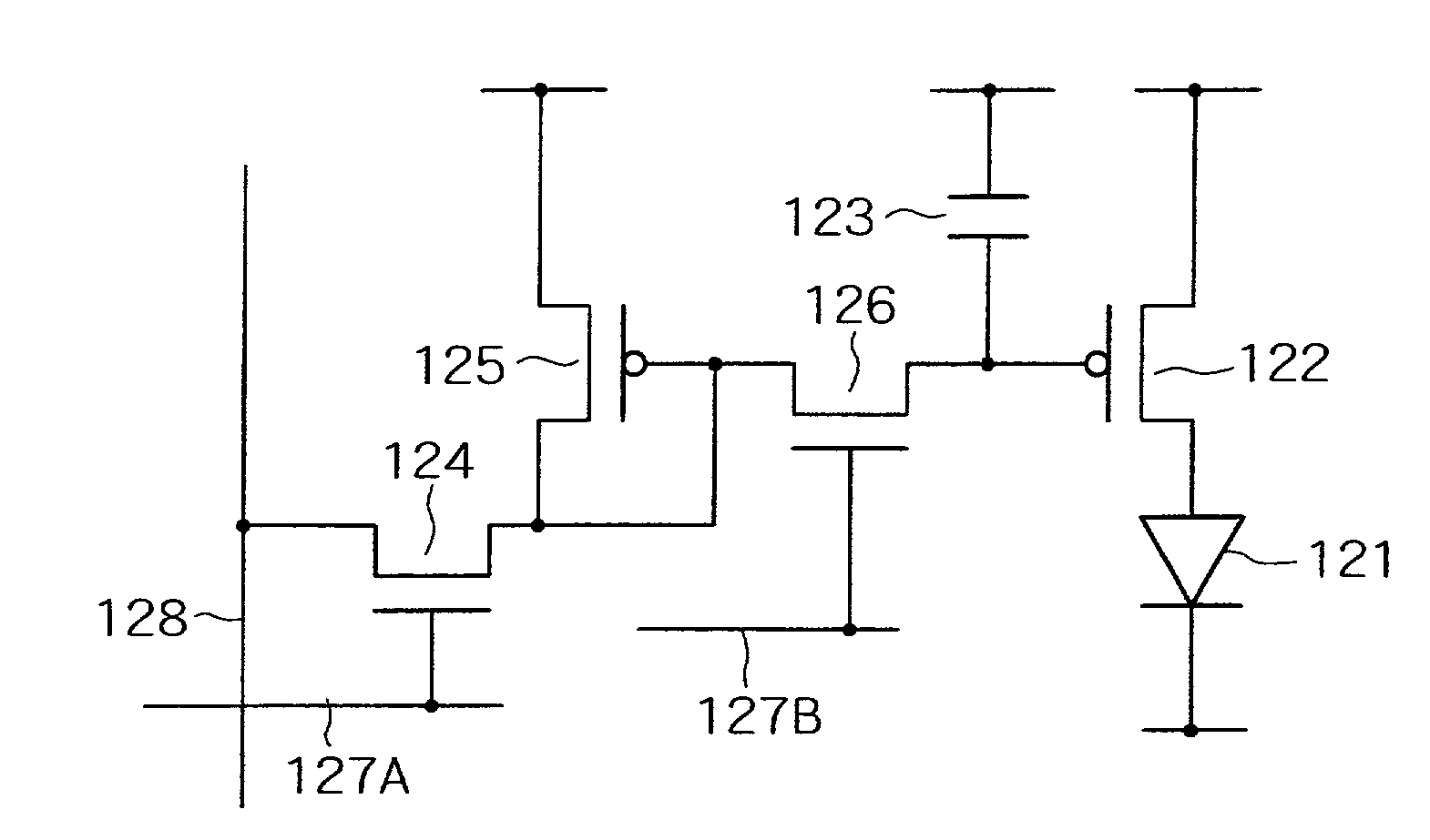
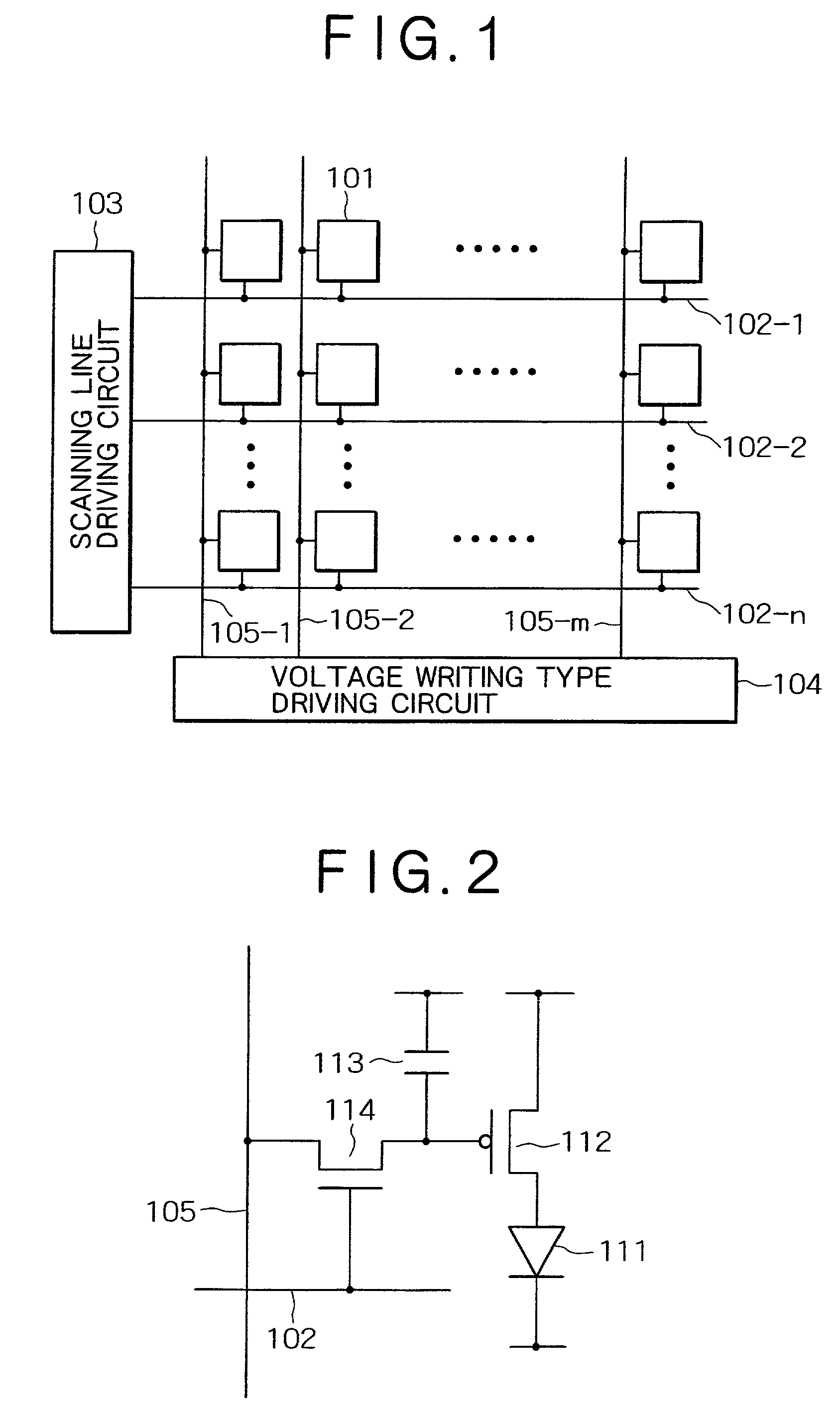
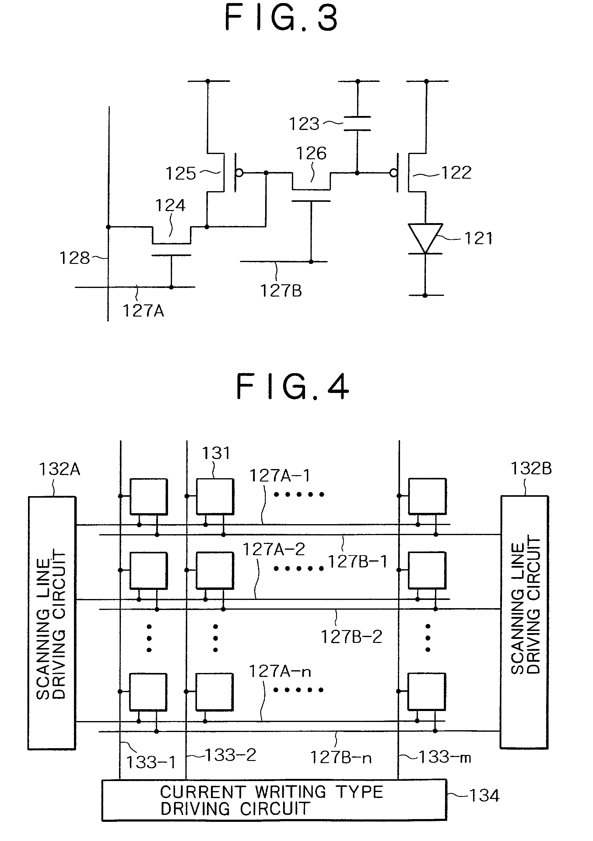
[0050]In FIG. 7, current writing type pixel circuits 11 corresponding in number with m columns×n rows are arranged in a matrix manner. First scanning lines 12A-1 to 12A-n and second scanning lines 12B-1 to 12B-n are both arranged one for each of the rows of the pixel circuits 11. A first scanning line driving circuit 13A is provided on a left side of the pixel unit to drive the first scanning lines 12A-1 to 12A-n, wh...

second embodiment

[0067]An active matrix type display apparatus according to a second embodiment of the present invention will next be described. The active matrix type display apparatus according to the second embodiment uses a circuit configuration obtained by omitting the data current control circuits 16 in the active matrix type display apparatus according to the first embodiment as shown in FIG. 7, that is, the same configuration as the active matrix type display apparatus according to the conventional example as shown in FIG. 4.

[0068]With this configuration, the active matrix type display apparatus according to the second embodiment realizes the same function as that of the active matrix type display apparatus according to the first embodiment by using a pixel circuit to which no writing is being performed as a data current control circuit (bypass current). A driving method of the active matrix type display apparatus according to the second embodiment will be specifically described in the follo...

third embodiment

[0089]FIG. 15 is a schematic diagram of a configuration of an active matrix type display apparatus according to a third embodiment of the present invention.

[0090]As with the active matrix type display apparatus according to the second embodiment, the active matrix type display apparatus according to the third embodiment is configured so as to share a first scanning line WS between x pixel circuits in the same block when x pixel circuits continuous in the column direction are formed into one block and selected simultaneously, and a data current is written to one of the pixel circuits and the other pixel circuits are used as bypass current circuits.

[0091]As described above regarding the active matrix type display apparatus according to the second embodiment, when two pixel circuits in the same block are selected simultaneously, scanning lines WS of the driven circuits operate in the same manner, and therefore the scanning line WS can be shared in the same block. In the present example...


PUM


Abstract

An active matrix type organic EL display apparatus according to the present invention which apparatus uses current writing type pixel circuits is provided with a current control circuit for each of data lines connected to the pixel circuits. The current control circuit supplies part of a data line current to a pixel circuit as a bypass current. The current control circuit handles the bypass current of the data line current represented by (data line current=data current+bypass current). Thereby, the data line driving current can be set greater than the data current flowing through TFTs provided in the pixel circuit, thus reducing luminance data writing time. Also, when the writing time is set unchanged, transistor size of the TFTs provided in the pixel circuit can be reduced.

Description

RELATED APPLICATION DATA[0001]The present application claims priority to Japanese Application(s) No(s). P2001-163955 filed May 31, 2001, and P2002-134918 filed May 10, 2002, which application(s) is / are incorporated herein by reference to the extent permitted by law.FIELD OF THE INVENTION[0002]The present invention relates to an active matrix type display apparatus having an active device in each pixel and controlling display in the pixel unit by means of the active device, and a driving method thereof, and particularly to an active matrix type organic EL display apparatus using an organic-material electroluminescence (hereinafter described as organic EL (electroluminescence)) device as an electrooptic device, and a driving method thereof.[0003]A liquid crystal display using a liquid crystal cell as a display device of a pixel, for example, has a large number of pixels arranged in a matrix manner, and controls light intensity in each pixel according to information of an image to be d...

Claims


Application Information

Patent Timeline
Patent Type & Authority Patents(United States)
IPC IPC(8): G09F9/30H01L51/50G09G3/20G09G3/30G09G3/32H01L27/32
CPCG09G3/3241G09G2300/0417G09G2300/0804G09G2300/0814G09G2300/0842G09G2310/0262G09G2320/0223G09G2320/0252G09G3/30
Inventor ASANO, MITSURU
Owner SONY CORP
Why Eureka
Try Eureka