In situ feature height measurement

a technology of feature height and measurement, applied in the field of in situ feature height measurement, can solve the problems of poor definition of structures, exacerbated problems, and formation of topographical irregularities on the wafer surfa

Inactive Publication Date: 2005-12-20
REVASUM INC +1
View PDF19 Cites 22 Cited by
  • Summary
  • Abstract
  • Description
  • Claims
  • Application Information

AI Technical Summary

Benefits of technology

[0011]The present invention achieves these benefits in the context of known process technology and known techniques in the art. The present invention provides an improved planarization apparatus for performing a planarization process, such as chemical mechanical planarization (CMP). Specifically, the present invention provides an improved planarization apparatus that provides multi-action CMP, such as orbital and spin action, and in situ monitoring and real-time feedback control to achieve uniformity during planarization. A planarization method for planarizing an object, such as a CMP process, comprises polishing a surface of the object to be planarized, and optically measuring feature heights of features on the surface of the object to obtain measurement data during said polishing of the surface.

Problems solved by technology

During IC manufacturing, the various masking and processing steps typically result in the formation of topographical irregularities on the wafer surface.
This problem is exacerbated by the use of multilevel interconnects.
A wafer surface that is not sufficiently planar, will result in structures that are poorly defined, with the circuits either being nonfunctional or, at best, exhibiting less than optimum performance.
However, it is commonly accepted that it still remains very difficult to obtain smooth results near the center of the wafer.
The result is a planarized wafer whose center region may or may not be suitable for subsequent processing.
Sometimes, therefore, it is not possible to fully utilize the entire surface of the wafer.
This reduces yield and subsequently increases the per-chip manufacturing cost.
Ultimately, the consumer suffers from higher prices.

Method used


Image

  • In situ feature height measurement
  • In situ feature height measurement
  • In situ feature height measurement

Examples


Embodiment Construction

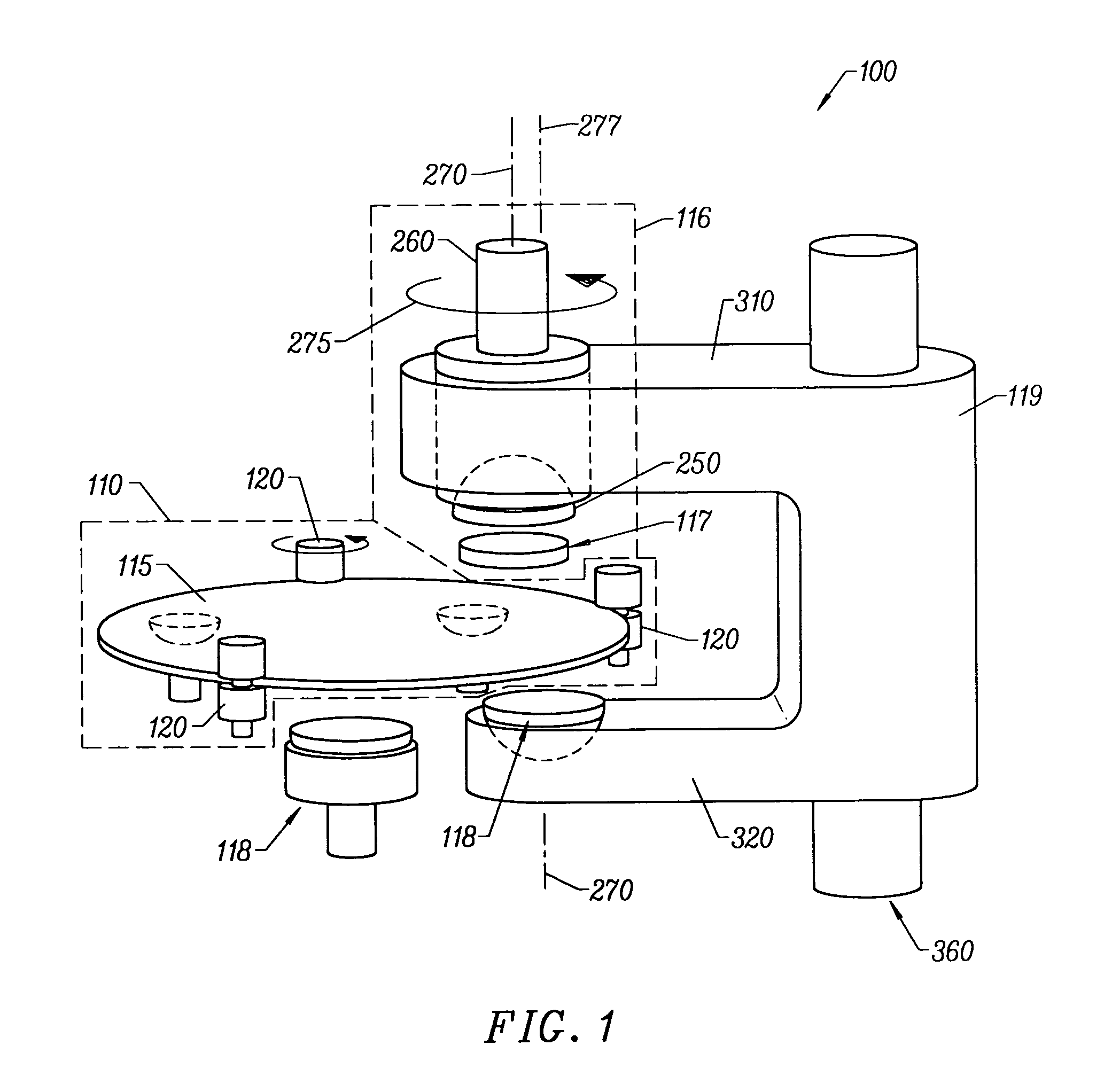
[0042]FIG. 1 is a simplified diagram of a planarization apparatus 100 according to an embodiment of the present invention. In this apparatus 100, the polishing pad is smaller, typically substantially smaller, in surface area than the substrate being planarized. Such an apparatus is referred to herein as a sub-aperture apparatus. The term full-aperture is used to describe a planarization apparatus in which the polishing pad is larger in surface area than the substrate being planarized. The diagram of FIG. 1 is merely an example, which should not limit the scope of the claims herein. One of ordinary skill in the art would recognize many other variations, modifications, and alternatives. In a specific embodiment, planarization apparatus 100 is a chemical-mechanical planarization apparatus.

Wafer Guide and Spin Assembly

[0043]The apparatus 100 includes an edge support, or a guide and spin assembly 110, that couples to the edge of an object, or a wafer 115. While the object in this specifi...


PUM

PropertyMeasurementUnit
angleaaaaaaaaaa
diameteraaaaaaaaaa
diameteraaaaaaaaaa

Abstract

Embodiments of the invention provide methods and apparatus for in situ feature height measurement of an object being planarized. In one embodiment, a method of planarizing an object comprises polishing a surface of the object to be planarized using a polishing pad having a cavity; and directing an incident light from the cavity of the polishing pad to optically measure feature heights of surface features on the surface of the object to obtain measurement data during the polishing of the surface using the polishing pad. The feature heights are relative height differences of the features measured by directing the incident light at the surface of the object from the cavity and observing a reflected light intensity of a reflected light from the features on the surface to the cavity.

Description

CROSS-REFERENCES TO RELATED APPLICATIONS[0001]This application is a continuation-in-part of U.S. patent application Ser. No. 09 / 699,290, filed Oct. 26, 2000 (now U.S. Pat. No. 6,629,874), which claims the benefit of U.S. Provisional Patent Application Nos. 60 / 161,705, 60 / 161,830, and 60 / 161,707, filed Oct. 27, 1999, and 60 / 163,696 filed Nov. 5, 1999. This application is also a continuation-in-part of U.S. patent application Ser. No. 10 / 216,107, filed Aug. 8, 2002, which is a continuation-in-part of U.S. patent application Ser. No. 10 / 146,494, filed May 14, 2002. The entire disclosures of the above patent applications are incorporated herein by reference.BACKGROUND OF THE INVENTION[0002]The present invention relates to the manufacture of electronic devices. More particularly, the invention provides a device for planarizing a film of material of an article such as a semiconductor wafer. In an exemplary embodiment, the present invention provides an improved substrate support for the ma...

Claims


Application Information

Patent Timeline
Patent Type & Authority Patents(United States)
IPC IPC(8): B24B37/04
CPCB24B37/04
Inventor HALLEY, DAVID G.BARBOUR, GREG
Owner REVASUM INC
Why Eureka
Try Eureka