Substrate for carrying a semiconductor chip and semiconductor device using same

a technology of semiconductor chips and substrates, applied in semiconductor devices, semiconductor/solid-state device details, electrical apparatus, etc., can solve the problems of reducing becoming too narrow, and reducing the availability of etching process capabilities, so as to reduce the arrangement pitch and increase the density of the arrangement of lands.

Inactive Publication Date: 2005-12-20
TEXAS INSTR INC
View PDF2 Cites 2 Cited by
  • Summary
  • Abstract
  • Description
  • Claims
  • Application Information

AI Technical Summary

Benefits of technology

[0010]In this way, because the constricted portion and capillary tool contact portion of the adjacent lands are arranged facing each other, the required gap between adjacent lands (the gap needed to enable etching processing) is guaranteed, and the region for preventing mutual contact between conductor wires is preserved, while the arrangement pitch of the lands can be reduced. As a result, it is possible to reduce the arrangement pitch and to increase the arrangement density of the lands.

Problems solved by technology

However, when the arrangement pitch of lands 930 is reduced, the following problems arise.
However, in this case, gap C between lands 930 becomes too narrow, and manufacturing becomes difficult using the present available etching process capability (which requires a gap of 30 μm or larger).
This is undesirable.

Method used


Image

  • Substrate for carrying a semiconductor chip and semiconductor device using same
  • Substrate for carrying a semiconductor chip and semiconductor device using same
  • Substrate for carrying a semiconductor chip and semiconductor device using same

Examples


Embodiment Construction

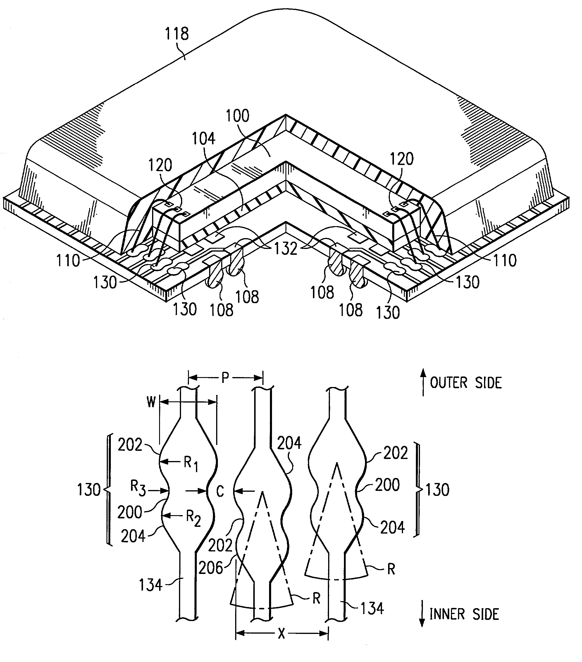
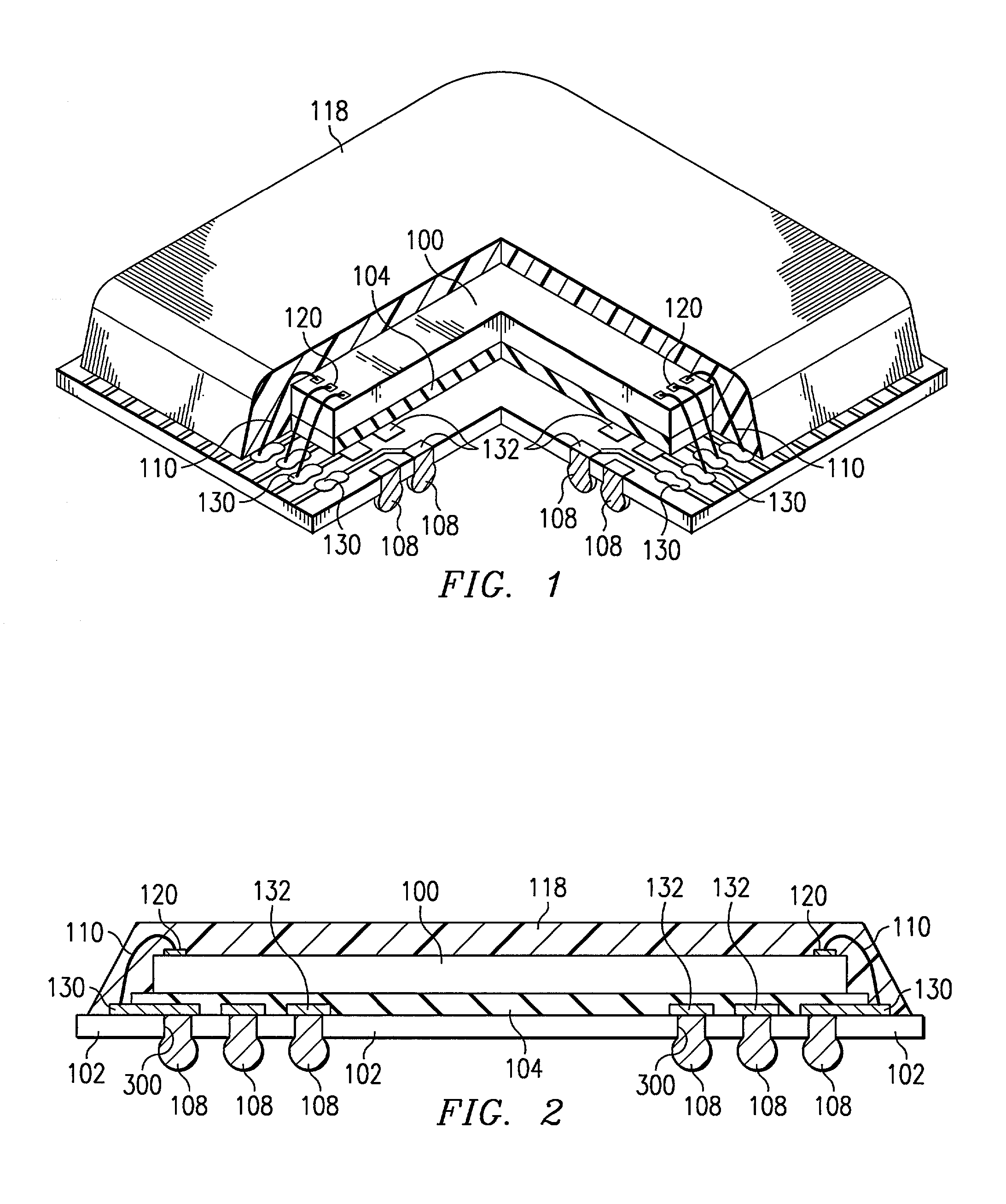
[0030]In the following, an embodiment of this invention will be explained with reference to figures. FIGS. 1 and 2 are a partially cutaway oblique view and a side cross section of the semiconductor package in this invention, respectively. For the semiconductor package in this embodiment, semiconductor chip 100 is attached by means of die bonding paste 104 to insulating substrate 102, and is sealed with sealant 118. For semiconductor chip 100, an integrated circuit not shown in the figure is formed on one side of a silicon substrate, and the other side is attached to insulating substrate 102. Plural electrode pads 120 led out from the integrated circuit are arranged on the outer periphery of the surface of semiconductor chip 100 on the integrated circuit side.

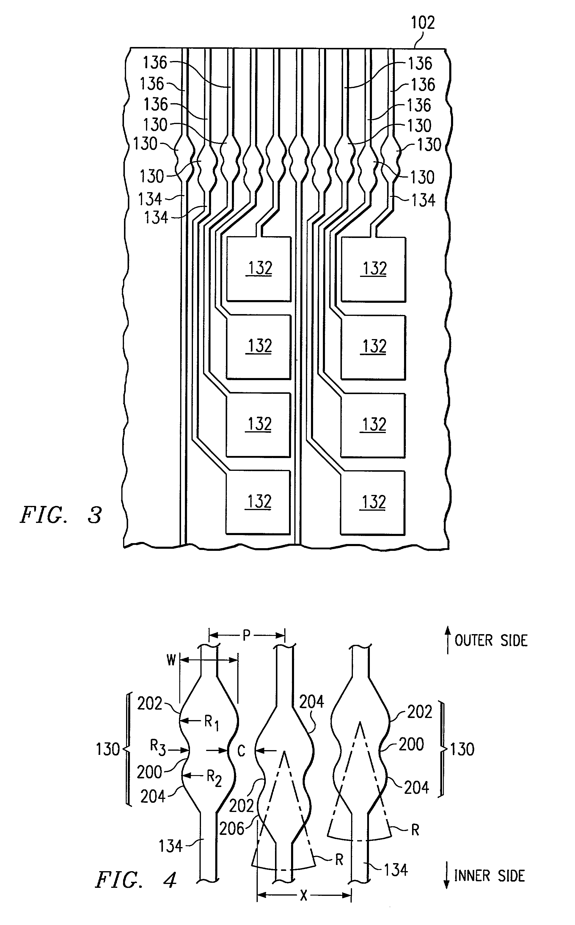
[0031]Insulating substrate 102 is a substrate made of polyimide or ceramics. On the surface of insulating substrate 102 (the surface on the side toward semiconductor chip 100), a conductor pattern is formed for making electrical...


PUM


Abstract

The objective of this invention is to provide a type of substrate for carrying a semiconductor chip that can increase the arrangement density of lands, and a type of semiconductor device that makes use of said substrate for carrying a semiconductor chip. Constitution: The conductor pattern on insulating substrate 102 contains lands 130 that are respectively connected to electrode pads 120 of semiconductor chip 100 via conductor wires 110. Each land 130 of conductor pattern 110 as capillary tool contact portion 202 where the capillary tool makes contact during bonding, and wire contact portion 204 that allows contact of conductor wire 110. The portion of wire contact portion 204 on the side toward capillary tool contact portion 202 becomes constricted portion 200. Lands 130 are positioned such that constricted portion 200 and capillary tool contact portion 202 of adjacent lands 130 are arranged facing each other.

Description

FIELD OF THE INVENTION[0001]This invention pertains to a type of substrate for carrying a semiconductor chip used in a semiconductor package or other semiconductor device, as well as a type of semiconductor device having said substrate for carrying a semiconductor.[0002]This application claims priority from Japanese patent application number 13(2001)-249908, filed Aug. 21, 2001.BACKGROUND OF THE INVENTION[0003]In recent years, with progress in miniaturization and performance upgrades of electronic information equipment, great efforts have been made to develop technology for increasing the density of semiconductor packages and of other semiconductor devices mounted on them. The BGA (Ball Grid Array) structure is a structure for increasing the density of semiconductor packages. FIG. 10 is a diagram illustrating an example of the basic constitution of a semiconductor package adopting a BGA structure. In this semiconductor package, semiconductor chip 900 having an integrated circuit for...

Claims


Application Information

Patent Timeline
Patent Type & Authority Patents(United States)
IPC IPC(8): H01L23/12H01L23/498
CPCH01L23/49838H01L24/32H01L24/49H01L24/85H01L24/45H01L24/78H01L2224/32057H01L2224/32225H01L2224/45124H01L2224/45144H01L2224/48091H01L2224/48227H01L2224/48465H01L2224/49433H01L2224/73265H01L2224/78301H01L2224/83385H01L2224/85181H01L2224/92247H01L2924/01004H01L2924/01005H01L2924/01006H01L2924/01013H01L2924/01014H01L2924/01015H01L2924/01028H01L2924/01029H01L2924/01074H01L2924/01078H01L2924/01079H01L2924/01082H01L2924/14H01L2924/15183H01L2924/15311H01L2924/00014H01L2924/01033H01L2924/014H01L24/48H01L2924/00012H01L2924/00H01L2924/12041H01L24/73H01L2224/05554H01L2224/45015H01L2924/10162H01L2924/181
Inventor ANO, KAZUAKI
Owner TEXAS INSTR INC
Why Eureka
Try Eureka