Planar optical waveguide vibrating sensor chip cantilever beam manufacturing method

A planar optical waveguide and vibration sensor technology, applied in instruments, using wave/particle radiation, measuring ultrasonic/sonic/infrasonic waves, etc., can solve the incompatibility of connection and packaging processes, the inability to prepare optical waveguide cantilever beam structures, and the mechanical strength of silicon materials lower problem

Inactive Publication Date: 2014-07-30
HARBIN INST OF TECH AT WEIHAI
View PDF3 Cites 4 Cited by
  • Summary
  • Abstract
  • Description
  • Claims
  • Application Information

AI Technical Summary

Problems solved by technology

However, the silicon material has low mechanical strength and is easy to damage, and the silicon etching method can only process small-sized cantilever beams, which are generally on the order of hundreds of nm to several μm. Low frequency band responds to mechanical vibration
For the optical waveguide chip on the glass substrate, the optical waveguide cantilever beam structure cannot be prepared by pure ...

Method used


Image

  • Planar optical waveguide vibrating sensor chip cantilever beam manufacturing method
  • Planar optical waveguide vibrating sensor chip cantilever beam manufacturing method
  • Planar optical waveguide vibrating sensor chip cantilever beam manufacturing method

Examples


Embodiment Construction

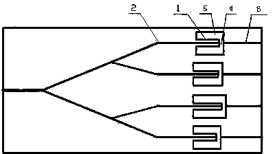
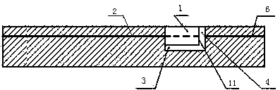
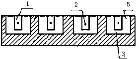
[0016] A method for manufacturing a planar optical waveguide vibration sensor chip cantilever beam, which uses a planar optical waveguide shunt chip on a glass substrate as a base material, and the planar optical waveguide shunt chip has an input shunt optical waveguide 2, an output shunt Optical waveguide 6; where the upper interface of the waveguide core layer of the input branch optical waveguide 2 is about 40 microns away from the upper surface of the planar optical waveguide branch chip. First, clean the upper and lower surfaces of the planar optical waveguide shunt chip. The upper and lower surfaces of the planar optical waveguide shunt chip are cleaned by placing the planar optical waveguide shunt chip on the glass substrate in acetone, deionized water, and alcohol in sequence. , cleaned with an ultrasonic wave with a power of 40 watts, put it into a vacuum drying oven, and heated it at a constant temperature of 80°C for half an hour. After cooling, clean the upper and l...


PUM

PropertyMeasurementUnit
Thicknessaaaaaaaaaa
Widthaaaaaaaaaa

Abstract

Provided is a planar optical waveguide vibrating sensor chip cantilever beam manufacturing method. A water assisting femtosecond laser machining method is used for machining a cantilever beam on a planar optical waveguide splitter chip, a pair of equal-length longitudinal grooves is formed in the two sides of each input splitter optical waveguide strip in parallel in a digging mode respectively, then a bottom gap is formed below a core layer zone where the input splitter optical waveguide is placed in a cutting mode, so that longitudinal grooves in the two sides are communicated in the bottom, then a horizontal groove communicated with the longitudinal grooves in the two sides is formed in the front ends of the longitudinal grooves in the two sides in a digging mode, and the cantilever beam which can vibrate freely is formed in the middle zone defined by the longitudinal grooves, the horizontal groove and the bottom gap. The cantilever beam with large size can be machined, the size of the cantilever beam is at the micron magnitude order or the millimeter magnitude order, and a manufactured planar optical waveguide vibrating sensor chip can respond to high-frequency wave band mechanical vibration and low-frequency wave band mechanical vibration.

Description

technical field [0001] The invention relates to an optical waveguide vibration sensor, in particular to a method for manufacturing a planar optical waveguide vibration sensor chip cantilever beam. Background technique [0002] Traditional vibration sensors generally use electrical sensors, which are difficult to work in environments with strong electromagnetic interference, high temperature and humidity, and high pressure, and are not suitable for long-distance sensing. [0003] Optical waveguide vibration sensors have been used to overcome the shortcomings of electrical sensors, and the majority of optical waveguide vibration sensors are in the form of cantilever beams. The existing cantilever beam processing method is an etching method, usually silicon etching is performed on the optical waveguide structure based on the silicon substrate, and the optical waveguide cantilever beam structure is processed. However, the silicon material has low mechanical strength and is easy...

Claims


Application Information

Patent Timeline
IPC IPC(8): G01H9/00
Inventor 高仁喜孙正和夏正娜
Owner HARBIN INST OF TECH AT WEIHAI
Why Eureka
Try Eureka