Integrated spark gap device

a spark gap and integrated technology, applied in the field of spark gap devices, can solve the problems of large amount of energy to be released, inability to embed spark gap devices in ics, etc., and achieve the effects of low cost, small size of the device, and mass production

Active Publication Date: 2005-12-20
AUBURN UNIV
View PDF6 Cites 42 Cited by
  • Summary
  • Abstract
  • Description
  • Claims
  • Application Information

AI Technical Summary

Benefits of technology

[0010]The integrated spark gap device of the present invention has many advantages over existing spark gap devices. One of the advantages of the integrated spark gap device of the present invention is that, because IC batch processing techniques can be used to produce the device, the device can be mass produced at very low cost. This is not the case with known EBW and some slapper devices, which are made of discrete components that must be assembled. Another advantage of the spark gap device of the present invention results from the very small size of the device. The IC package that contains the device can be inserted directly into the explosive fill of munitions or into warheads. Because no additional room is required for the spark gap device, munitions can be reduced in size. This size reduction can have many beneficial effects, including, for example, an increase in the number of ordinates that can be carried on an aircraft. Another advantage is that multiple IC packages containing the spark gap devices can be inserted into the explosive fill to provide multi-point detonation capabilities.

Problems solved by technology

To date, it has not been feasible to embed spark gap devices in ICs because discharging a very large voltage over a very small area on an IC over a clock cycle causes a very large amount of energy to be released, which will essentially vaporize the IC.

Method used


Image

  • Integrated spark gap device
  • Integrated spark gap device
  • Integrated spark gap device

Examples


Embodiment Construction

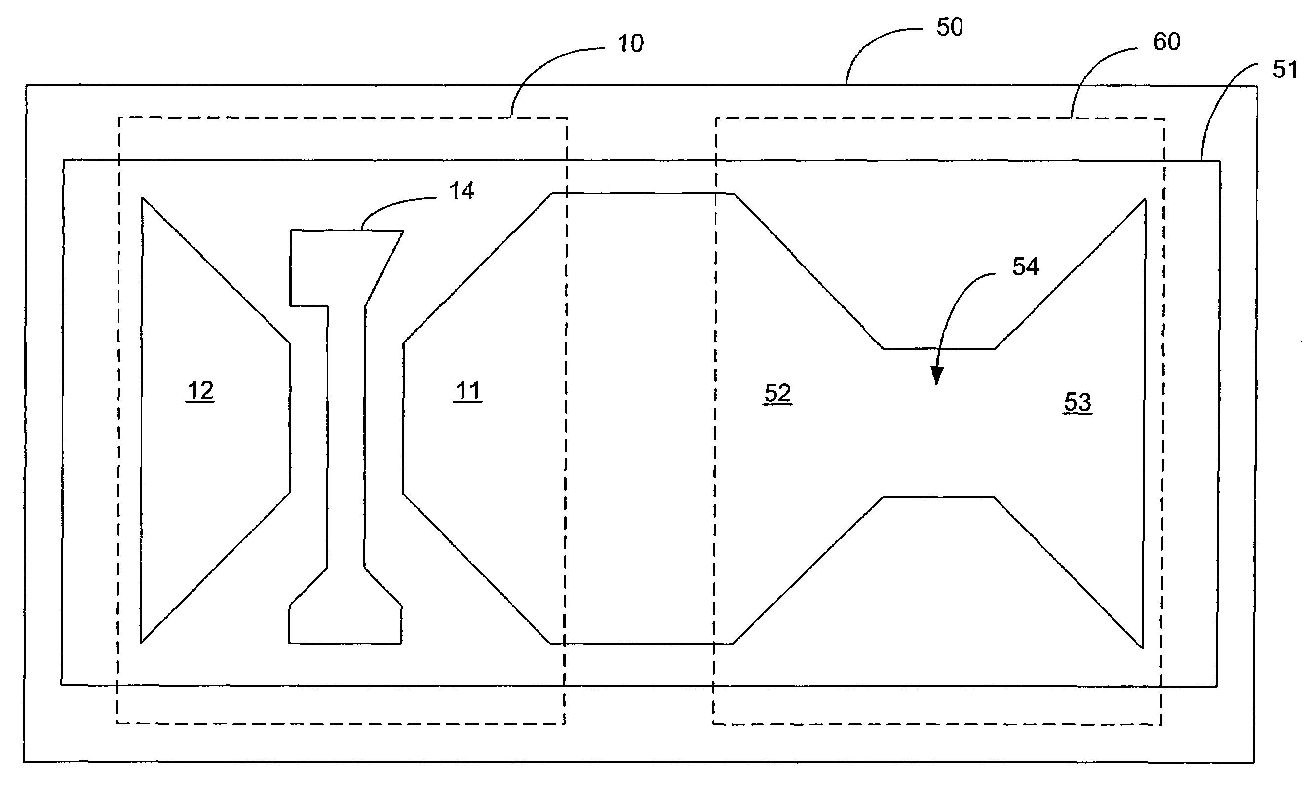
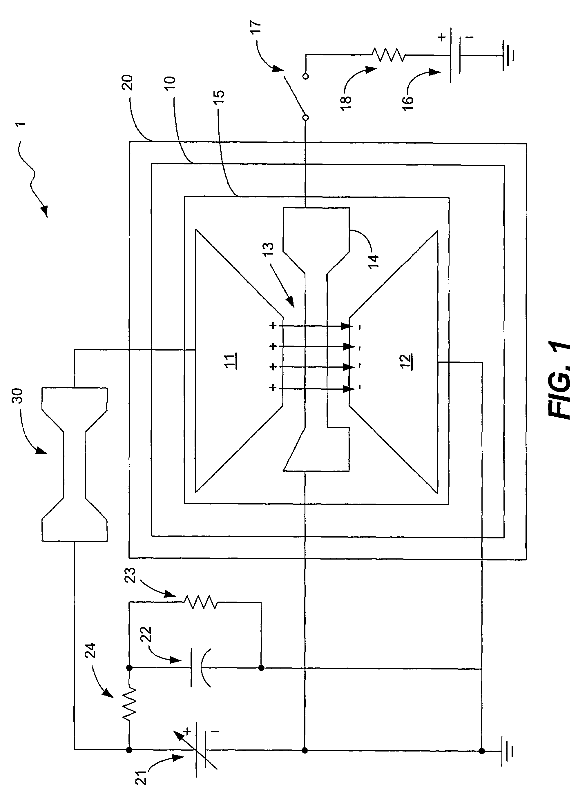
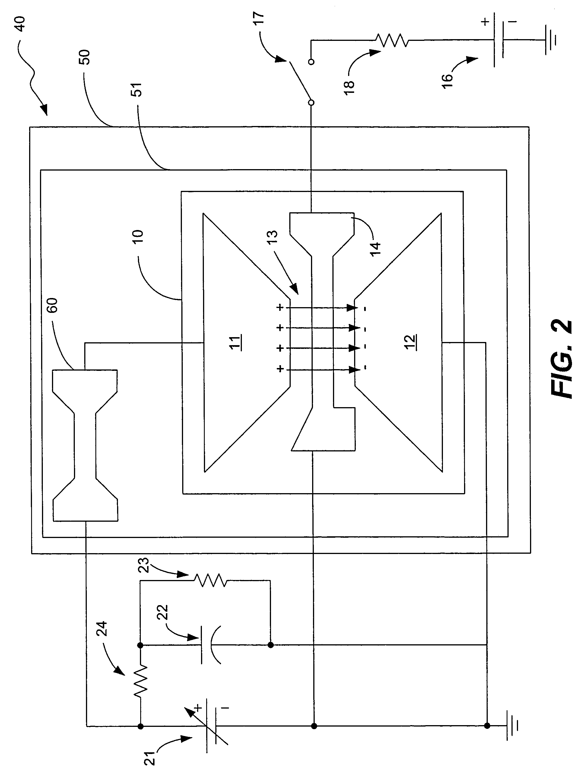
[0016]The present invention is a spark gap device that is capable of operating at high voltages and that is fabricated on an integrated circuit (IC). The term “integrated circuit”, as that term is used herein, is intended to denote a circuit comprising components that are integrated together on a substrate material. The substrate material is not limited to any particular type of material. FIG. 1 illustrates a plan view of a schematic diagram of the integrated spark gap device 1 of the present invention in accordance with an embodiment. The layout shown in FIG. 1 is one of many possible layouts that can be used for the integrated spark gap device 1. The present invention is not limited to any particular IC layout for the spark gap device.

[0017]In accordance with the embodiment shown in FIG. 1, the integrated spark gap device comprises a high-voltage switch 10 formed on a substrate material 20. In accordance with this embodiment, the substrate material 20 is a dielectric material such...


PUM

PropertyMeasurementUnit
voltageaaaaaaaaaa
conductiveaaaaaaaaaa
electric fieldaaaaaaaaaa

Abstract

A spark gap device that is formed in an integrated circuit (IC). The IC has a dielectric substrate upon which a high-voltage switch is disposed. The switch includes an anode element and a cathode element separated from each other by a spark gap. A trigger electrode is disposed on the substrate material in the spark gap. A capacitor is electrically coupled to the trigger electrode. The cathode and anode elements and the trigger electrode preferably are at least partially covered with a dielectric material. When the capacitor is charged, the charge on the capacitor exerts a strong electric field on the cathode and anode elements that causes ions to migrate in the cathode and anode elements toward the spark gap. When the trigger electrode is excited by an electrical current, the ions arc across the gap and a conductive path is created between the cathode element and the anode element.

Description

CROSS-REFERENCE TO RELATED APPLICATIONS[0001]The present application claims the benefit of priority to provisional application Ser. No. 60 / 444,433, filed on Feb. 3, 2003, entitled “TRIGGERED HIGH-VOLTAGE SWITCH”, which is incorporated herein by reference in its entirety.TECHNICAL FIELD OF THE INVENTION[0002]The present invention relates to spark gap devices, and more particularly, to a spark gap device comprising an integrated circuit (IC).BACKGROUND OF THE INVENTION[0003]Spark gap devices are used to generate large electrical discharges. They typically include a dielectric cylinder, which is often made of a ceramic material such as alumina, an anode on one end of the cylinder, a cathode on the other end of the cylinder and a dielectric material between the anode and cathode that electrically isolates the anode and cathode from each other. The dielectric material is typically a gas, such as argon or nitrogen, or a vacuum. When a large enough potential difference is created across th...

Claims


Application Information

Patent Timeline
Patent Type & Authority Patents(United States)
IPC IPC(8): H01J17/30H01J17/46H01T2/02
CPCH01J17/46H01T2/02
Inventor BAGINSKI, THOMAS A.
Owner AUBURN UNIV
Why Eureka
Try Eureka