Event driven dynamic logic for reducing power consumption

a dynamic logic and power consumption technology, applied in the field of digital logic circuitry, can solve the problems of increasing clock signal loading, requiring higher power clock sources and additional discharging, and increasing circuit power consumption by repetitive charging and discharging, so as to reduce capacitive loading and reduce power consumption. , the effect of reducing power consumption

Inactive Publication Date: 2005-12-20
RGT UNIV OF CALIFORNIA
View PDF4 Cites 27 Cited by
  • Summary
  • Abstract
  • Description
  • Claims
  • Application Information

AI Technical Summary

Benefits of technology

[0025]The present invention comprises a method and apparatus for reducing power consumption within digital logic circuits which may be utilized in combinatorial and / or sequential logic circuits. By way of example, and not of limitation, by reducing the relative activity of the clock input signal as applied to the clock inputs of the digital logic circuits, the capacitive loading is thereby reduced with attendant reductions in power consumption. The invention recognizes that logic circuits are typically only subject to changing output conditions for a small number of the given input and intermediary conditions for which a clock signal transition may be received.

Problems solved by technology

Consequently, circuit power consumption is increased by repetitive charging and discharging, even when no net circuit activity results.
Furthermore, clock signal loading can be substantially increased which requires higher power clock sources and additional dissipation.
One drawback of this static topology is that each input signal is gated to both PMOS and NMOS transistors, thereby subjecting the inputs to large gate load capacitances and their associated charge delays.
However, dynamic logic circuits are subject to high power consumption levels.
As a result, power is consumed unnecessarily by the clock without any circuit operation for fifteen out of the sixteen possible input combinations.
Unfortunately, the substantial power losses which arise within the dynamic logic circuits as a consequence of repetitive charging and discharging make the circuit generally less desirable for these applications.
As a result, a substantial percentage of the operating power is unnecessarily consumed by the unproductive activity of clock signal CLK 74, which is subject to loading even when no desired circuit state changes occur.
It has been shown that both combinatorial and sequential logic circuits are similarly subject to capacitive loading of the clock signal, wherein circuit power is consumed even when no net (productive) circuit activity is occurring.

Method used


Image

  • Event driven dynamic logic for reducing power consumption
  • Event driven dynamic logic for reducing power consumption
  • Event driven dynamic logic for reducing power consumption

Examples


Embodiment Construction

[0056]Referring more specifically to the drawings, for illustrative purposes the present invention is embodied in the apparatus generally shown in FIG. 4 through FIG. 9. It will be appreciated that the apparatus may vary as to configuration and as to details of the parts, and that the method may vary as to the specific steps and sequence, without departing from the basic concepts as disclosed herein.

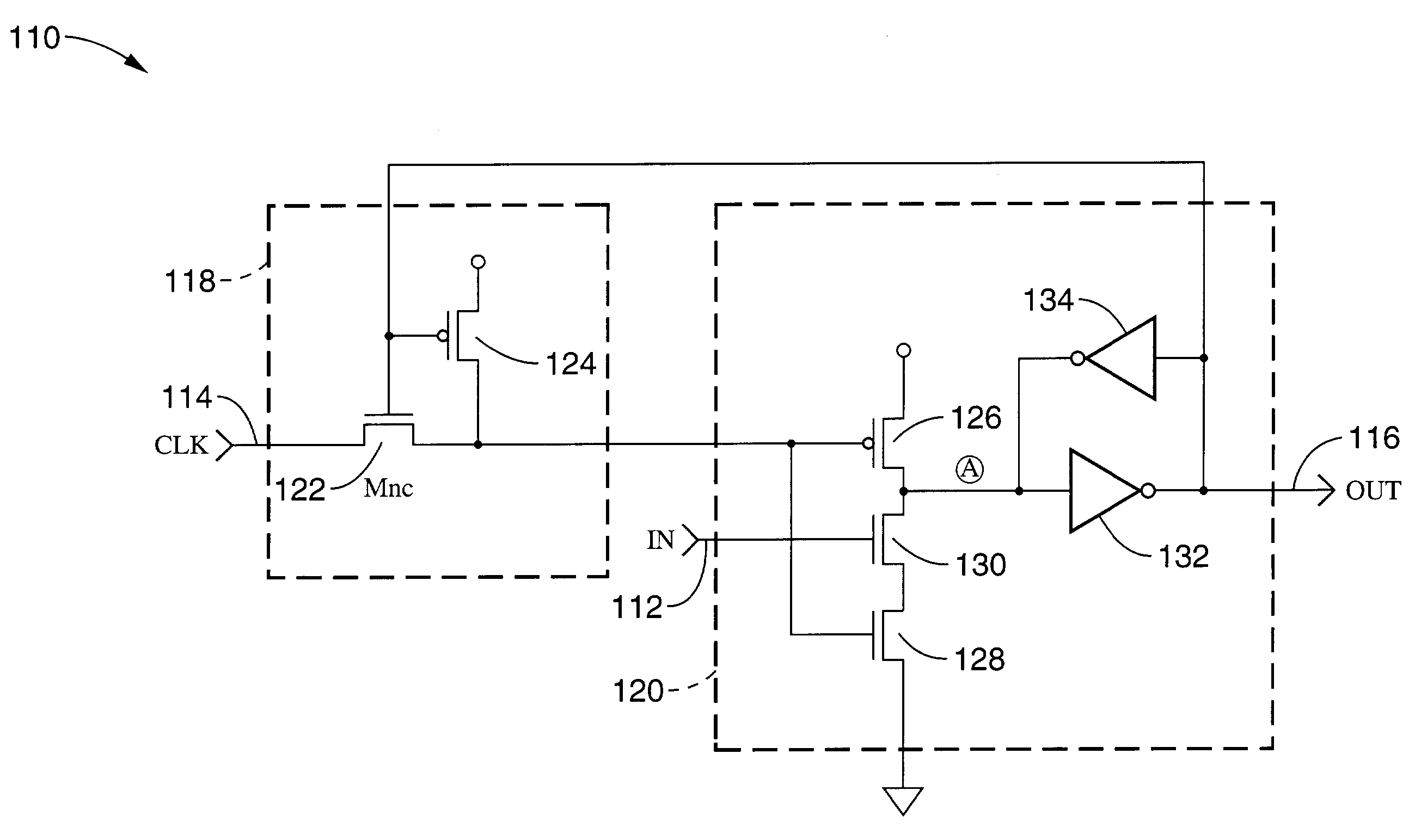
[0057]FIG. 4 exemplifies a one input event driven logic circuit 110, similar to the four input AND domino combinatorial logic circuit shown in FIG. 2. Logic circuit 110 has a logic input 112, clock input 114, and output 116. A clock path control circuit 118 is shown for selectively blocking clock signal 114 from a generally conventional dynamic logic circuit 120 in response to a true logic evaluation.

[0058]The general operation of the present method involves cycling the logic circuit through clock phases which include precharge and evaluation phases while an active clock signal is being ...


PUM


Abstract

Methods and circuits are described for reducing power consumption within digital logic circuits by blocking the passage of clock signal transitions to the logic circuits when the clock signal would not produce a desired change of state within the logic circuit, such as at inputs, intermediary nodes, outputs, or combinations. By way of example, the incoming clock is blocked if a given set of logic inputs will not result in an output change of state if a clock signal transition were to be received. By way of further example, the incoming clock is blocked in a data flip-flop if the input signal matches the output signal, such that receipt of a clock transition would not produce a desired change of state in the latched output. The invention may be utilized for creating lower power combinatorial and/or sequential logic circuit stages subject to less unproductive charging and discharging of gate capacitances.

Description

CROSS-REFERENCE TO RELATED APPLICATIONS[0001]This application claims priority from U.S. provisional application Ser. No. 60 / 408,407 filed on Sep. 3, 2002, incorporated herein by reference.STATEMENT REGARDING FEDERALLY SPONSORED RESEARCH OR DEVELOPMENT[0002]Not ApplicableREFERENCE TO A COMPUTER PROGRAM APPENDIX[0003]Not ApplicableBACKGROUND OF THE INVENTION[0004]1. Field of the Invention[0005]This invention pertains generally to digital logic circuitry, and more particularly to reducing power consumption using event driven logic wherein the clock signal is only propagated within the circuit after a true logic operation is performed.[0006]2. Description of the Background Art[0007]Conventional logic circuitry often utilizes a clock signal which is received by various levels of gating within the circuitry for synchronizing the state changes within the circuitry so as to eliminate race conditions and other similar problems. As a result, the clock signal is applied to a number of gates wi...

Claims


Application Information

Patent Timeline
Patent Type & Authority Patents(United States)
IPC IPC(8): H03K3/012H03K19/00H03K19/096
CPCH03K3/012H03K19/0963H03K19/0016H03K19/096H03K19/20
Inventor KANG, SUNG-MOYOO, SEUNG-MOON
Owner RGT UNIV OF CALIFORNIA
Why Eureka
Try Eureka