
Wafer-level package with silicon gasket

a silicon gasket and wafer-level technology, applied in the direction of fluid speed measurement, instruments, microstructured devices, etc., can solve the problems of prone to deformation, low permeability of deposited materials, and high humidity, and achieve less force and/or time to bond, and facilitate uniform tightness

Inactive Publication Date: 2005-12-27
AVAGO TECH INT SALES PTE LTD
View PDF3 Cites 34 Cited by
  • Summary
  • Abstract
  • Description
  • Claims
  • Application Information

AI Technical Summary

Benefits of technology

[0005]In accordance with an illustrated preferred embodiment of the present invention, a gasket for a wafer-level package is carved out from the wafer material itself. The wafer is typically made of silicon, although materials such as glass, 3–5 compounds, ceramics, plastics or other materials can be used. Silicon is extremely rigid, and therefore an ideal gasket material. When pressure is applied during bonding, the silicon gasket will not deform, and the applied pressure is concentrated at the bond juncture. As a result, it takes less force and / or time to bond the wafer-level package. Furthermore, the original wafer surface is manufactured to be extremely flat. Since the gasket surface is the original wafer surface, the gasket will also have an extremely flat surface, which facilitates a uniformly tight bond.
[0006]The present invention also uses existing silicon etching technology that offers high precision in both etch depth and gasket width when carving out the desired shape. This allows greater control over the dimensions of the hermetically sealed cavity. Also, due to the high strength of silicon, the gaskets can be made narrower than in the past—usually no more than 10 um wide. The surface area of the gasket determines the amount of pressure on the bond juncture during bonding for a given bonding force. Since a narrower gasket has less surface area, it is able to concentrate more of the applied bonding force at the bond juncture to create a strong seal.

Problems solved by technology

Many semiconductor devices are sensitive to contamination, humidity, and other such environmental factors.
However, the deposited material is not very rigid, and is prone to deformation when pressure is applied during the bonding process.
Furthermore, the process of depositing material creates an irregular gasket bonding surface, which causes problems during bonding.
Finally, it is difficult to precisely control the geometry of the gasket, since the deposited material tends to shrink or change shape during the deposition process.

Method used


Image

  • Wafer-level package with silicon gasket
  • Wafer-level package with silicon gasket
  • Wafer-level package with silicon gasket

Examples


Embodiment Construction

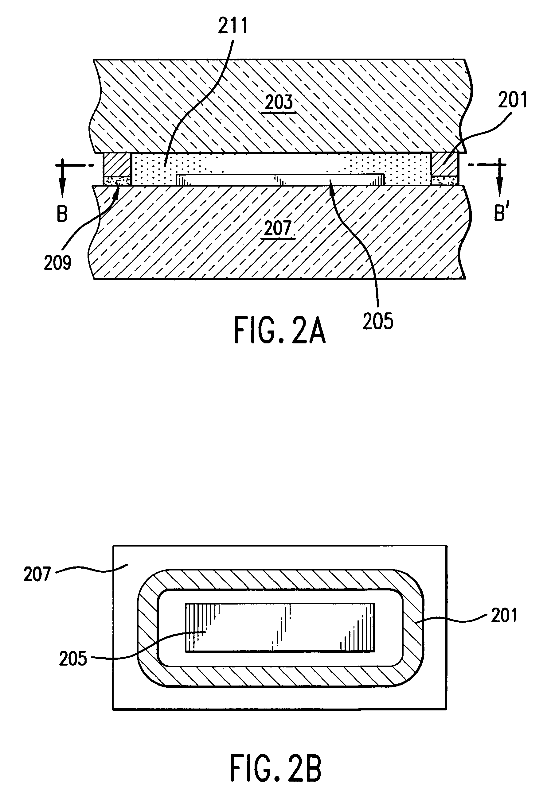
[0014]FIG. 2A shows a cross-sectional view of a preferred embodiment made in accordance with the teachings of the present invention. A gasket 201 on a cap wafer 203 surrounds and seals off a device 205 fabricated on a base wafer 207. Device 205 is any microelectronic device such as a microelectromechanical system (MEMS) structure or electronic circuit. Typically, the wafers are made of silicon. The wafers can also be made of glass, ceramics, or other semiconductor material, without departing from the scope of the present invention.

[0015]FIG. 2B shows a top-down view of the present invention, taken along the line B–B′ in FIG. 2A. As can be seen more clearly in FIG. 2B, gasket 201 completely surrounds and encloses device 205. Although gasket 201 is shown as an oblong, gasket 201 can be a square, circle, oval, rectangle, or any other shape that will enclose device 205.

[0016]Referring back to FIG. 2A, gasket 201 is carved or etched out of cap wafer 203 and bonded to base wafer 207 with ...


PUM


Abstract

A gasket encloses a hermetically sealed environment between a cap wafer and a base wafer. The gasket is bonded to the base wafer using bonding material. The bonding material can be one or more of many substances that exhibit acceptable adhesion, sealing, and other properties that ensure a hermetically sealed environment. The gasket is carved out from the cap wafer material itself. The cap wafer is typically made of extremely strong and rigid material such as silicon. Since the gasket is made from the cap wafer, the gasket itself is also extremely strong and rigid.

Description

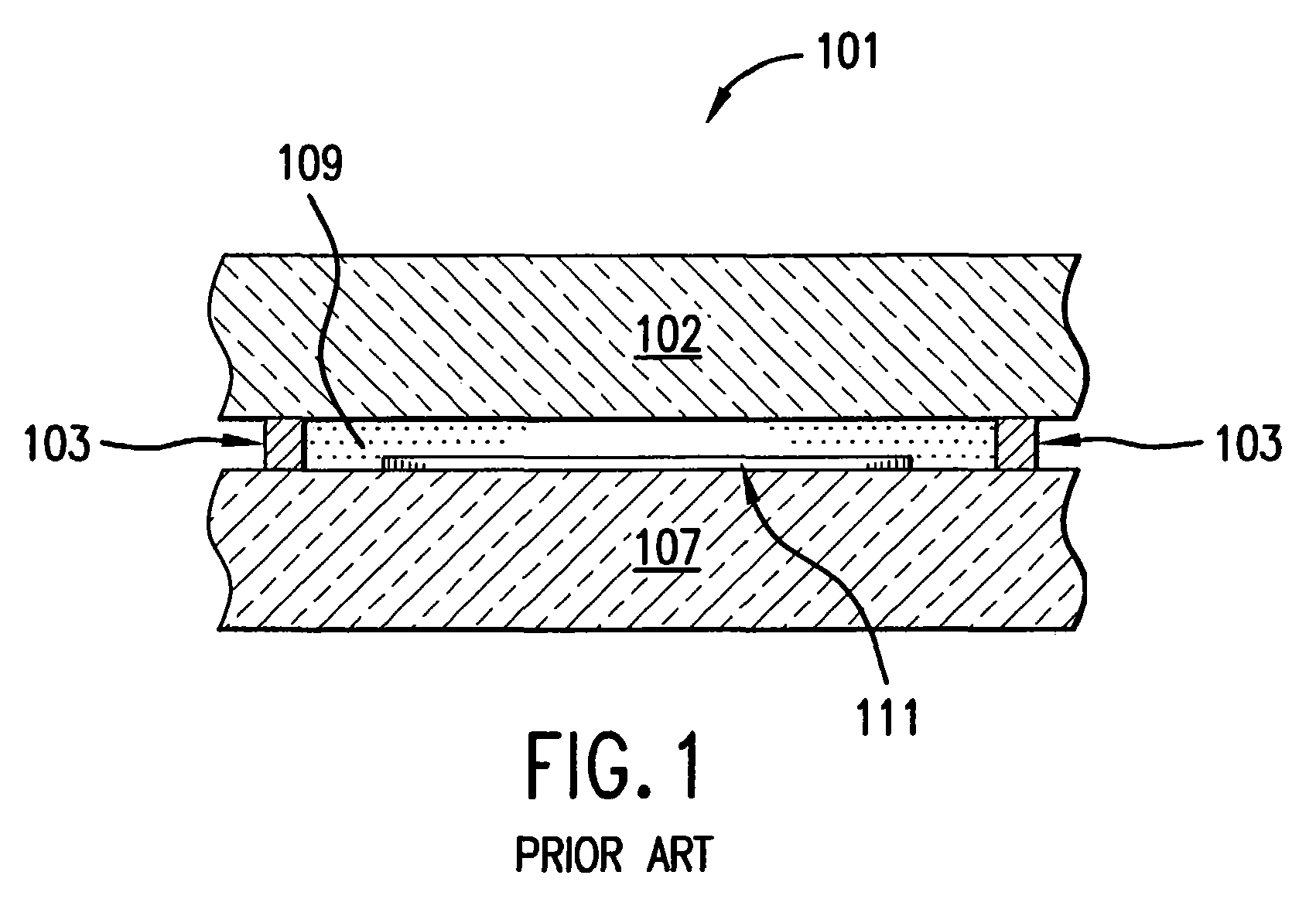
[0001]This is a Divisional of application Ser. No. 10 / 028058, filed on Dec. 20, 2001 now U.S. Pat. No. 6,787,897, the entire disclosure of which is incorporated herein by reference.FIELD OF THE INVENTION[0002]The present invention is directed towards semiconductor packaging techniques, and more specifically, towards the fabrication of wafer-level packages.BACKGROUND OF THE INVENTION[0003]Many semiconductor devices are sensitive to contamination, humidity, and other such environmental factors. To protect them from harm, the devices must be put in a hermetically sealed package. In the past, a device had to first be cut or otherwise separated from its wafer before it could be put into a package. In wafer-level packaging, packaging is performed while the device remains on the wafer. In this fashion, hundreds or thousands of packages can be created simultaneously, and then separated by sawing or other means.[0004]FIG. 1 illustrates an exemplary wafer-level package 101. A first wafer 102 ...

Claims


Application Information

Patent Timeline
Patent Type & Authority Patents(United States)
IPC IPC(8): H01L23/02B81B7/00H01L21/50H01L23/10
CPCB81B7/0077H01L21/50H01L23/10H01L2924/01079H01L2924/09701H01L2924/0002H01L2924/00
Inventor GEEFAY, FRANK SGAN, QINGMATTOS, ANNFIGUEREDO, DOMINGO A
Owner AVAGO TECH INT SALES PTE LTD
Learn More