Methodology for a MEMS variable optical attenuator

a variable optical attenuator and microelectromechanical technology, applied in the field of microelectromechanical systems (mems) attenuators, can solve the problems of limiting the use of variable optical attenuators (voas) to long-haul optical telecommunications networks, limiting the yield of these components, and limiting the use of low-index contrast silica-on-silicon platforms. , to achieve the effect of simplifying the network,

Inactive Publication Date: 2005-12-27
XEROX CORP
View PDF17 Cites 34 Cited by
  • Summary
  • Abstract
  • Description
  • Claims
  • Application Information

AI Technical Summary

Benefits of technology

[0005]The optical network is a natural evolution of point-to-point dense wavelength division multiplexing (DWDM) transport to a more dynamic, flexible, and intelligent networking architecture to improve service delivery time. The main element of the optical network is the wavelength (channel), which will be provisioned, configured, routed, attenuated and managed in the optical domain. Intelligent optical networking will be first deployed as an “opaque” network in which periodic optical-electrical conversion will be required to monitor and isolate signal impairments. Longer range, the optical network will evolve to a “transparent” optical network in which a signal is transported from its source to a destination entirely within the optical domain.
[0006]A key element of the emerging optical network is an optical add / drop multiplexer (OADM). An OADM will drop or add specific wavelength channels without affecting the through channels. Fixed OADMs can simplify the network and readily allow cost-effective DWDM migration from simple point-to-point topologies to fixed multi-point configurations. True dynamic OADM, in which reconfiguration is done in the optical domain without optical-electrical conversion, would allow dynamically reconfigurable, multi-point DWDM optical networks. This dynamically reconfigurable multi-point architecture is slated to be the next major phase in network evolution, with true OADM an enabling network element for this architecture.
[0007]On chip integration of optical switching and planar light circuits has the potential to greatly reduce the size and manufacturing costs of multi-component optical equipment such as Variable Optical Attenuators (VOAs). Current costs for Variable Optical Attenuators (VOAs) are significant, limiting their use to long-haul optical telecommunications networks. In order to extend their use into the metropolitan network the cost will need to be decreased by an order of magnitude without sacrificing performance.
[0008]One solution in particular to decreasing cost is through the integration of components, where the primary cost savings will be in packaging. A number of approaches are being pursued for optical integration using Planar Light Circuit (PLC) technologies. The majority of approaches use a silica-on-silicon platform with the VOA formed from the integration of silica Arrayed Waveguide Gratings (AWG's) for multiplexing and demultiplexing, with Thermo-Optic (TO) attenuators for performing the add / drop and pass of the demultiplexed signal. The use of a low-index contrast silica-on-silicon platform severely limits the yield of these components due to the requirement for uniform thick oxide films over large areas to form the waveguides. The use of TO attenuators limits the extensibility due to high-power requirements and thermal cross-talk.

Problems solved by technology

Current costs for Variable Optical Attenuators (VOAs) are significant, limiting their use to long-haul optical telecommunications networks.
The use of a low-index contrast silica-on-silicon platform severely limits the yield of these components due to the requirement for uniform thick oxide films over large areas to form the waveguides.
The use of TO attenuators limits the extensibility due to high-power requirements and thermal cross-talk.
While silica waveguides have optical properties that are well matched to the optical properties of conventional single mode fibers, and thus couple well to them, they require thick cladding layers due to the low index of refraction contrast between the waveguide core and cladding materials, making them difficult to fabricate using planar processing techniques for fabrication and integration with other on-chip optical devices.
The low index of refraction contrast, Δn, between core and cladding also requires large bending radii to limit optical loss during propagation through the photonic lightwave circuit, leading to large chip footprints and low die yields (<50%).
In addition, silica based waveguide attenuators are typically based on Mach-Zehnder interference using thermo-optic effects, that have a limited Extinction Ratio (ER) of around 25–30 dB, require significant power due to the low thermo-optic coefficient of silica, have problems with thermal cross-talk between the different optical channels and have a sinusoidal rather than a digital optical response.

Method used


Image

  • Methodology for a MEMS variable optical attenuator
  • Methodology for a MEMS variable optical attenuator
  • Methodology for a MEMS variable optical attenuator

Examples


Embodiment Construction

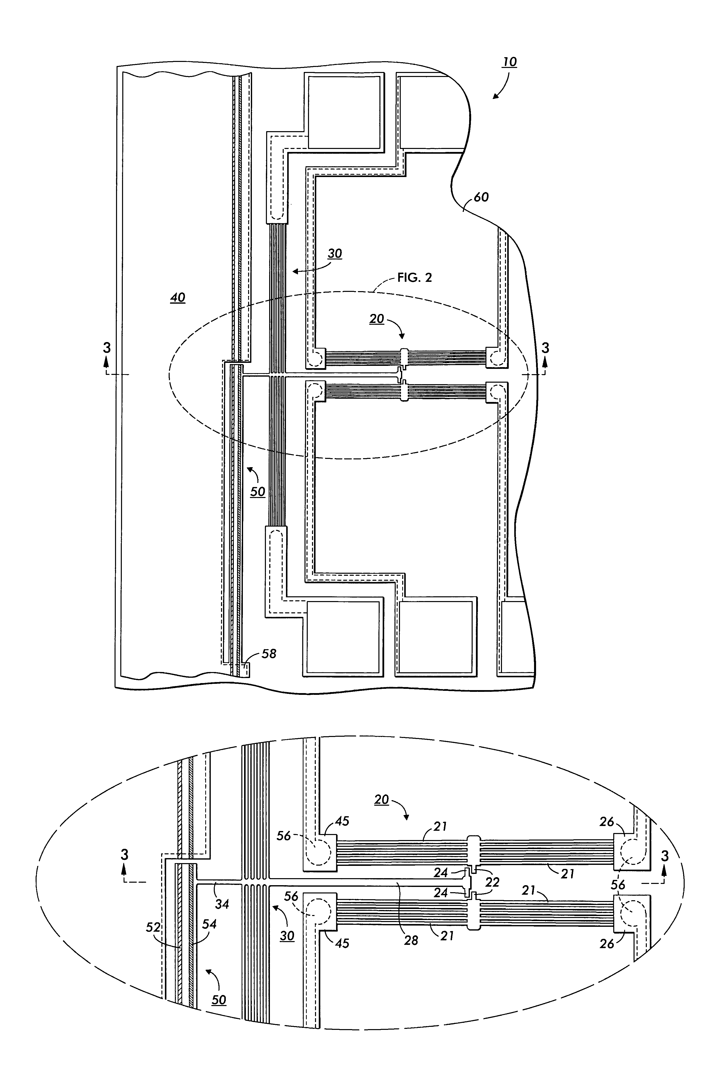
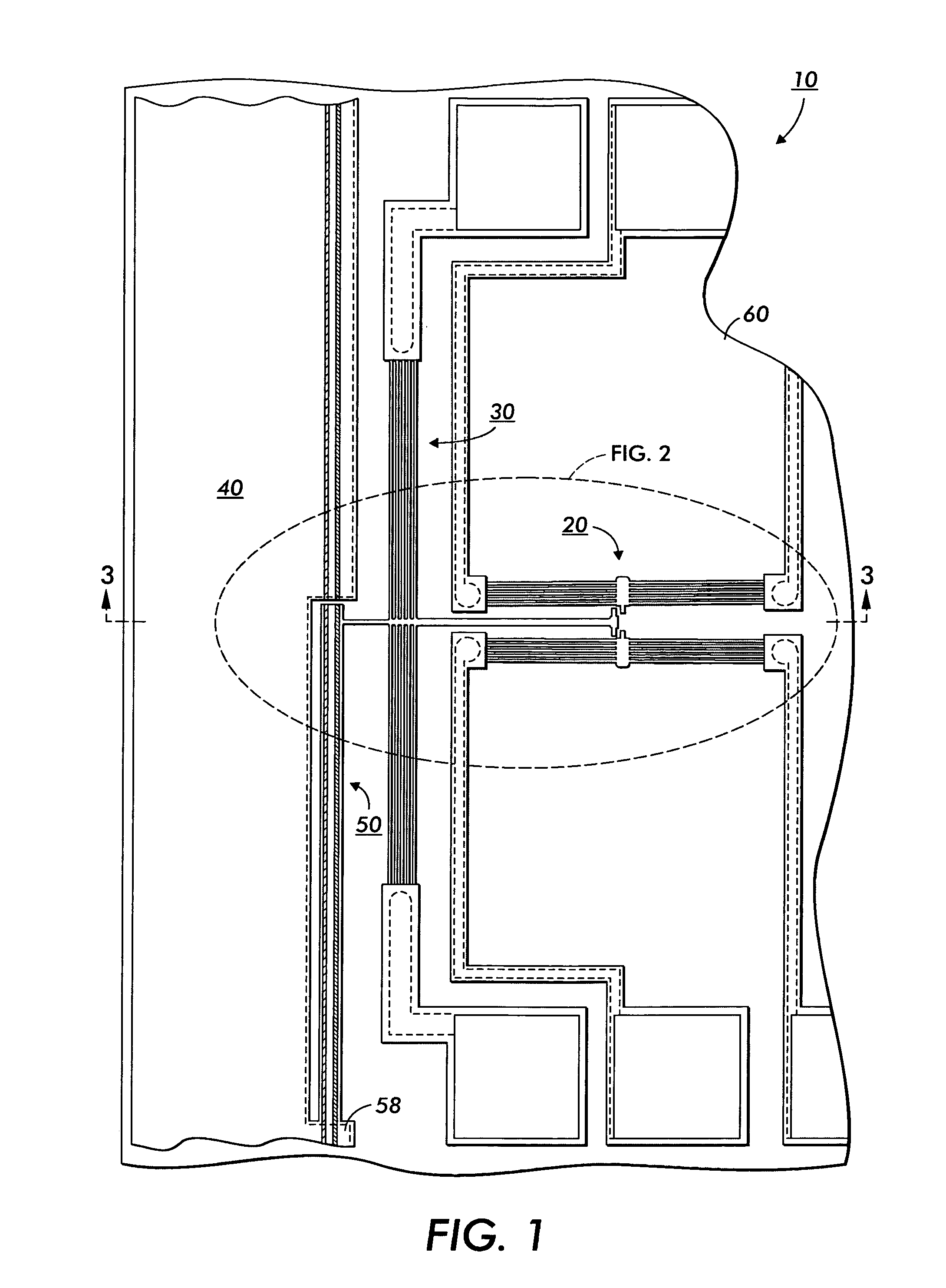
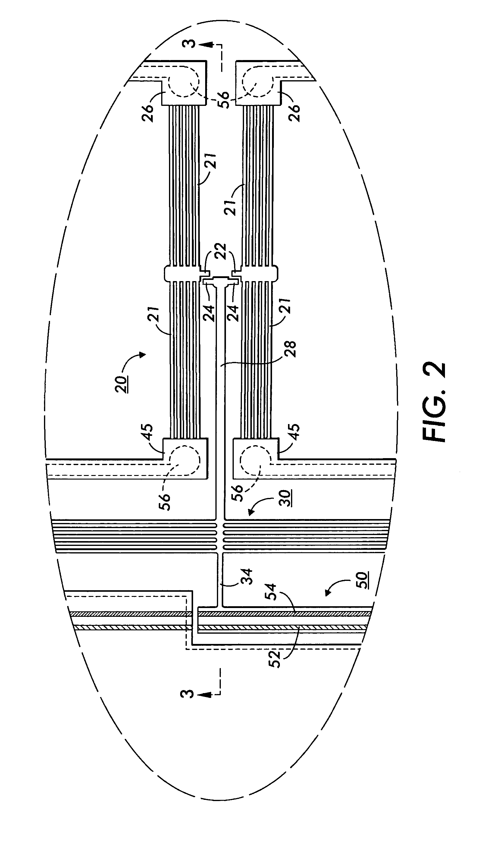
[0044]The teaching as provided herein below provides for an improved cantilever beam optical switch design which provides the function of switching and also performs the function of a variable optical attenuator (VOA). After the optical switching of a movable waveguide associated with the cantilever beam optical switch, a small degree of intentional misalignment of the movable waveguide will create different levels of optical attenuation. By finely controlling the misalignment of a selected switched position, the device can thereby provide the functions of both switching and attenuating. This exemplary integration of the switching function and the VOA function also reduce the optical loss which is otherwise unavoidable when the inevitable alterative of a separate switch and a separate VOA must necessarily be employed. This improved device can also be applied for correcting the difference in optical intensity created by the manufacturing tolerances inherent in the fabrication of an a...


PUM


Abstract

An improved cantilever beam optical switch methodology which provides the function of a variable optical attenuator (VOA). A small degree of intentional misalignment of the waveguide will create different levels of optical attenuation. By finely controlling the misalignment of a selected switched position, a single device may be realized that will provide the functions of both switching and attenuating or just attenuation alone. The optical MEMS device utilizes a latching mechanism in association with a thermal drive actuator for aligning a cantilever beam platform. The integration of the switching function and the VOA function reduce the optical loss which is otherwise unavoidable when the inevitable alterative of a separate switch and a separate VOA must necessarily be employed. The resultant improved device can also be applied for correcting the difference in optical intensity created by the manufacturing tolerances inherent in the fabrication of array waveguide gratings.

Description

CROSS-REFERENCE TO RELATED APPLICATIONS[0001]Cross reference is made to the following application filed concurrently herewith and incorporated by reference herein: U.S. application Ser. No. 11 / 010,769 entitled “Cantilever Beam MEMS Variable Optical Attenuator”. Attention is directed to copending applications U.S. Publication No. 2004 / 0184720, published Sep. 23, 2004, entitled, “M×N Cantilever Beam Optical Waveguide Switch”, U.S. Publication No. 2004 / 0184709, published Sep. 23, 2004, entitled “MEMS Waveguide Shuttle Optical Latching Switch”, and U.S. Publication No. 2004 / 0184710, published Sep. 23, 2004, entitled, “MEMS Optical Latching Switch”. Attention is further directed to copending U.S. application Ser. No. 10 / 995,965, entitled “Microfabrication Process for Control of Waveguide Gap Size”. The disclosure found in each of these copending applications is hereby incorporated by reference in its entirety.BACKGROUND AND SUMMARY[0002]The embodiments disclosed herein relate generally t...

Claims


Application Information

Patent Timeline
Patent Type & Authority Patents(United States)
IPC IPC(8): G02B6/26G02B6/35
CPCG02B6/266
Inventor LIN, PINYENWANG, YAO RONGMA, JUN
Owner XEROX CORP
Why Eureka
Try Eureka