Memory bus termination with memory unit having termination control

a technology of memory bus and termination control, which is applied in the direction of electric digital data processing, instruments, computing, etc., can solve the problems of reducing the amount of energy reflected on the stub, increasing the probability that erroneous data will be sensed at the receiver,

Inactive Publication Date: 2005-12-27
TAHOE RES LTD
View PDF4 Cites 109 Cited by
  • Summary
  • Abstract
  • Description
  • Claims
  • Application Information

AI Technical Summary

Problems solved by technology

Electrically, each stub or drop is a potential source of noise on data bus 30, as signal reflections from stubs connected to idle memory units can reach the intended recipient of a data transfer out-of-phase with the original signaling, increasing the probability that erroneous data will be sensed at the receiver.
When enabled, each termination circuit absorbs signals propagating down its respective stub, thus diminishing the amount of energy reflected on that stub.

Method used


Image

  • Memory bus termination with memory unit having termination control
  • Memory bus termination with memory unit having termination control
  • Memory bus termination with memory unit having termination control

Examples


first embodiment

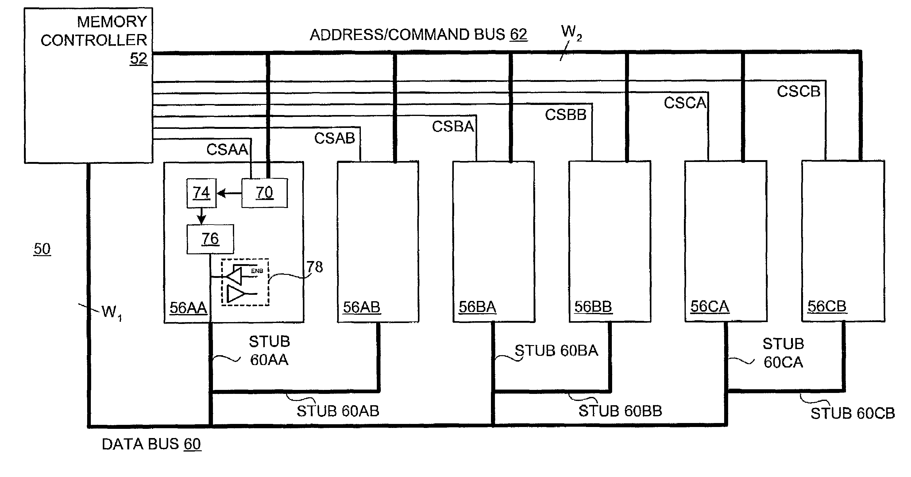
[0026]In a first embodiment, address / command decoder 70 and termination control logic 74 implement a state-based control scheme for controlling termination circuit 76. Each memory device (or rank of devices) is assumed to be in one of three states: IDLE, READ, or WRITE. The IDLE state indicates that the memory device is not in the process of performing a read or write on the data bus. The READ state indicates that the memory device is performing (or is about to perform) a read in which port 78 will drive data back to the controller across the data bus. The WRITE state indicates that the memory device is performing (or is about to perform) a write in which port 78 will receive data from the controller across the data bus. Address / command decoder 70 can easily include these states into its control circuitry, particularly since it produces similar signals during read and write operations in order to coordinate the operation of the memory core and data port with the data bus timing defi...

second embodiment

[0032]A second embodiment is illustrated in FIG. 7. In this embodiment, the memory controller embeds, within its address / command signals, information that identifies the memory unit, device, or rank selected for a particular read or write operation. For instance, with six ranks, six unique read commands (READn, where n identifies a rank between 0 and 5, inclusive) are defined. Likewise, six unique write commands, WRITEn, are defined. An address / command generator within the memory controller already determines which rank corresponds to a memory address supplied by a requesting host, in order to enable the proper chip select line. This determination can be used as well to select the READn command corresponding to the rank, and transmit READn instead of a generic READ.

[0033]The address / command decoder on each memory device decodes each read or write command issued by the memory controller, regardless of whether chip select has been asserted for that device. Thus for the third of six ra...


PUM


Abstract

Methods and apparatus for a memory system using line termination circuits in each memory unit (e.g., integrated circuit memory device) are disclosed. The memory unit contains termination control logic that sets the state of a controllable termination circuit to control reflections on the data bus. The termination control logic determines the proper state for the termination circuit from the state of its memory unit, and in some cases, from the approximate state of the data bus as gleaned from commands decoded from the command/address bus. A termination configuration register on the unit can be used to define the appropriate termination state for each unit state and/or data bus state.

Description

FIELD OF THE INVENTION[0001]This present invention relates generally to digital memory devices and systems, and more particularly to data bus termination and data bus termination control for such devices and systems.BACKGROUND OF THE INVENTION[0002]Microprocessors, digital signal processors, digital imaging devices, and many other types of digital data processing devices rely on an attached high-speed memory system to hold data and / or processor instructions needed by the processing device. As these processing devices become faster and more powerful, the increased demands placed on them generally translate to a need for larger and faster attached memory systems.[0003]FIG. 1 depicts a typical memory system configuration 20. A host processor 22 issues data store and retrieve requests to a memory controller 24 over a front-side bus FSB. Memory controller 24 acts as an intermediary for the exchange of data between processor 22 and memory units 26A, 26B, 26C, and 26D.[0004]Typical memory ...

Claims


Application Information

Patent Timeline
Patent Type & Authority Patents(United States)
IPC IPC(8): G06F13/40
CPCG06F13/4086
Inventor DODD, JAMES M.KHANDEKAR, NARENDRA S.
Owner TAHOE RES LTD
Why Eureka
Try Eureka