Fabrication process for a magnetic tunnel junction device

a tunnel junction device and fabrication process technology, applied in semiconductor devices, solid-state devices, instruments, etc., can solve the problems of high temperature stress experienced by the device, discharge of displaced particles during the process, damage to the device,

Inactive Publication Date: 2006-01-10
INFINEON TECH AG +1
View PDF12 Cites 106 Cited by
  • Summary
  • Abstract
  • Description
  • Claims
  • Application Information

AI Technical Summary

Problems solved by technology

Although RIE and ion milling provide the advantage of anisotropic (directional) removal of material, the main drawback of RIE and ion milling is the discharge of displaced particles being removed during the process, which can be projected in many different directions.
Another problem is that re-deposited conductive material may form a bridge between conducting lines, which should be avoided as well.
A major drawback of this method, however, is the high temperature stress experienced by the device.
Such high temperature stress can damage the device and / or negatively affect its performance abilities.
Other problems encountered using prior methods of forming an MTJ 30 include corrosion of copper lines and low etch selectivity for TiN hard masks, which are commonly used.

Method used


Image

  • Fabrication process for a magnetic tunnel junction device
  • Fabrication process for a magnetic tunnel junction device
  • Fabrication process for a magnetic tunnel junction device

Examples


first embodiment

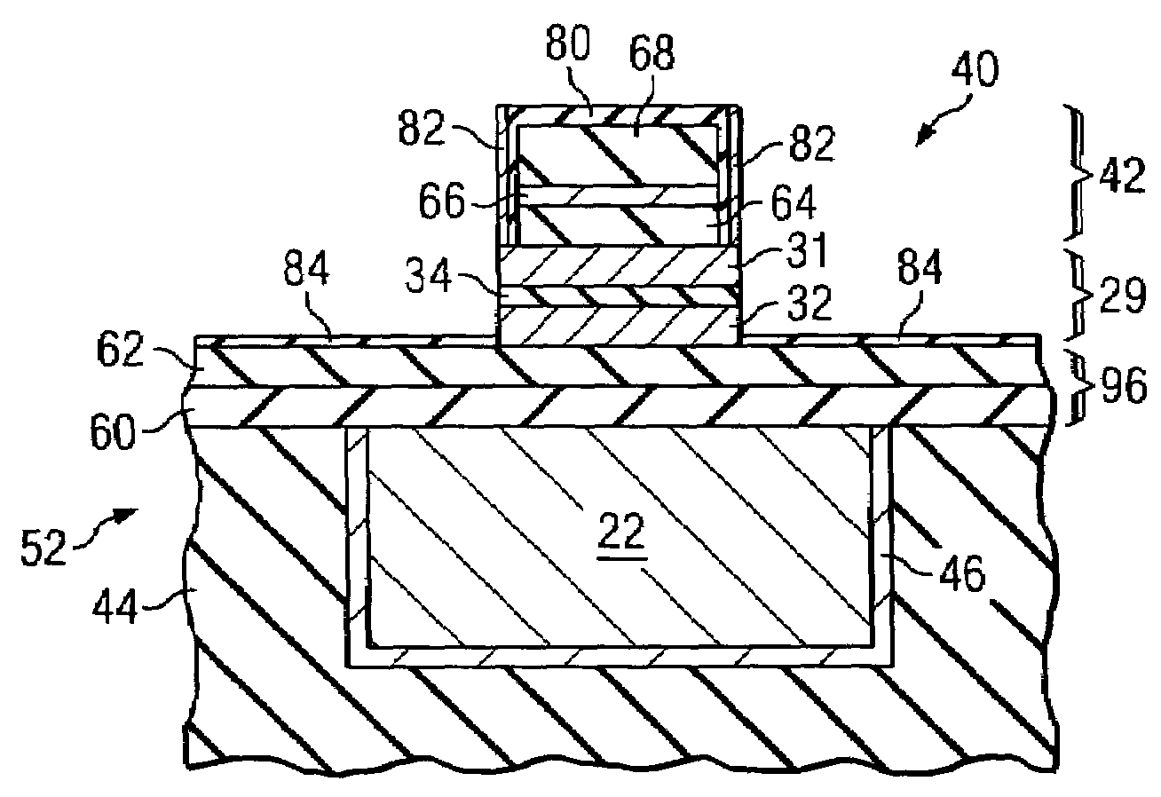
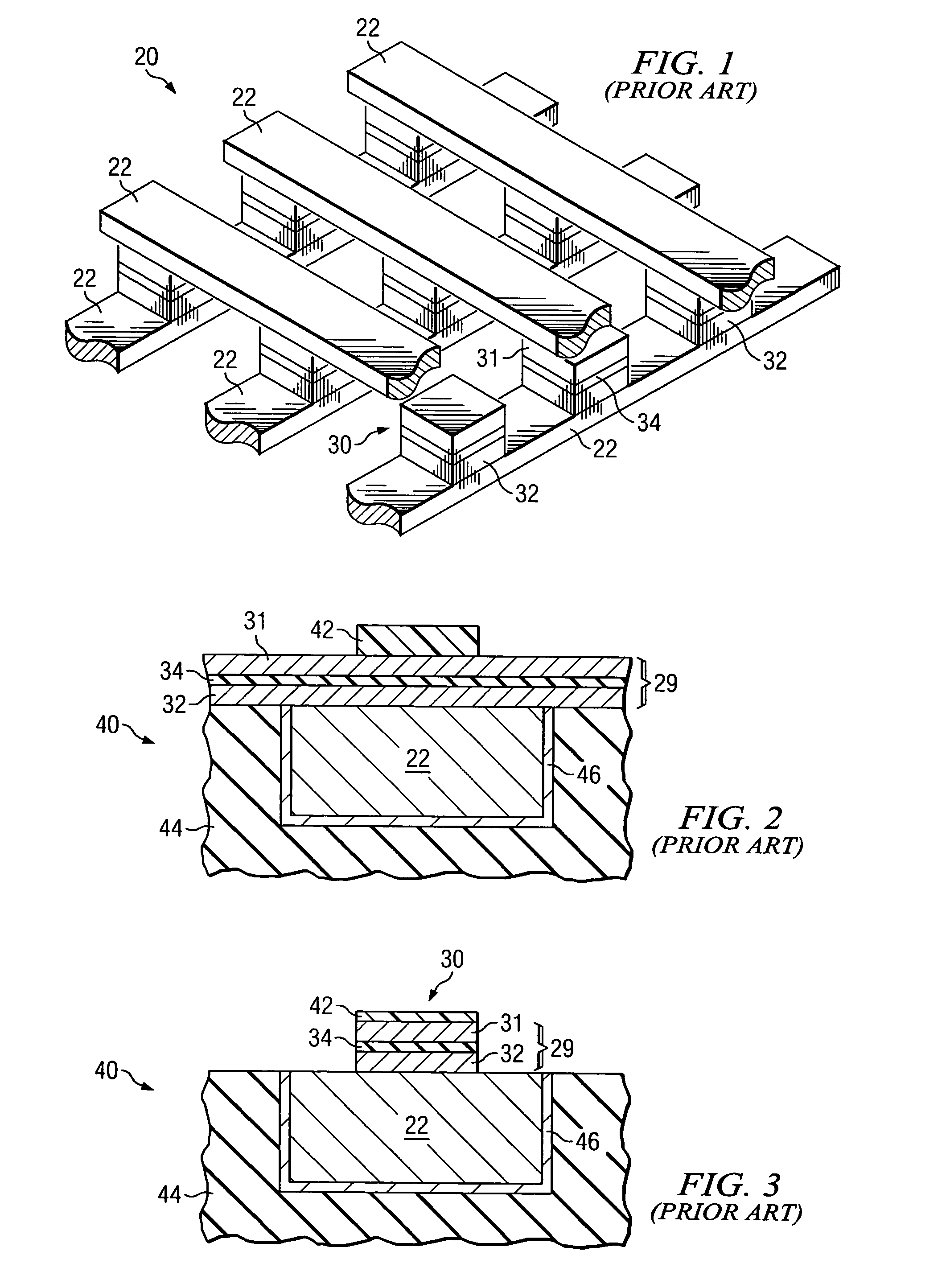
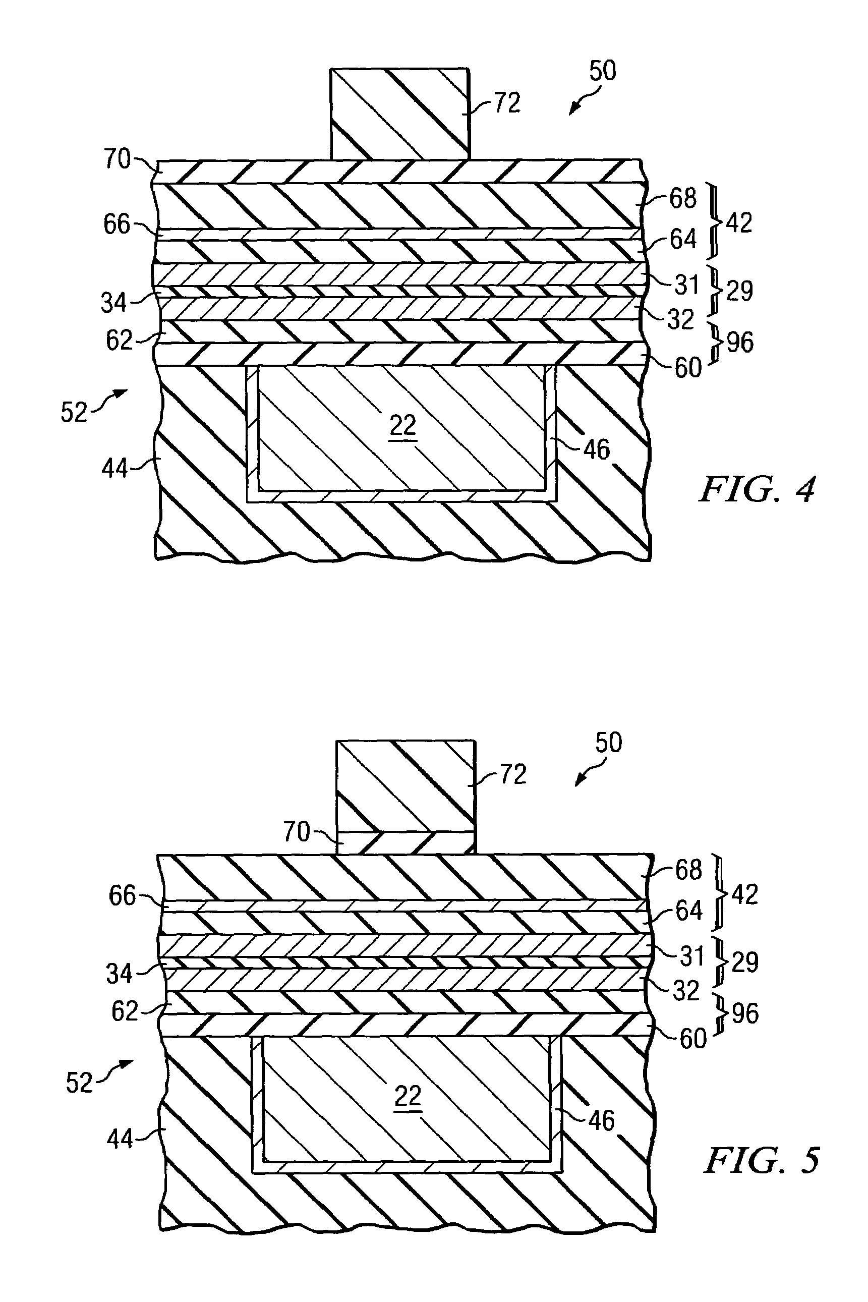
[0029]Still referring to FIG. 4, the initial structure 50 of the first embodiment includes a bottom tantalum nitride layer 60 over the underlying layer 52. A tantalum layer 62 is over the bottom tantalum nitride layer 60. An MTJ stack 29 is over the tantalum layer 62. A tantalum nitride cap layer 64 is over the MTJ stack 29. A titanium layer 66 is over the tantalum nitride cap layer 64. A titanium nitride layer 68 is over the titanium layer 66. An anti-reflective coating (ARC) layer 70 is over the titanium nitride layer 68. A patterned photoresist layer 72 is over the ARC layer 70. The photoresist layer 72 may be patterned using conventional methods, for example.

[0030]Tables 1 and 2 below provide illustrative process parameters that may be used for an embodiment of the present invention. Table 1 provides some preferred process parameters and conditions that may be used. The values provided in Table 1 are merely illustrative and these values may be varied thereabout to also provide p...

second embodiment

[0060]FIG. 18 shows the structure 50 after the ARC layer 70 is opened in alignment with the patterned photoresist layer 72. In the second embodiment, the hard mask 42 is etched and patterned completely before removing the photoresist layer 72, as shown in FIG. 19. As shown in FIG. 20, the sides of the hard mask 42 are plasma oxidized during (or during and after) the removal of the photoresist layer 72 (and the ARC layer 70) using an oxygen containing plasma, such as an O2 and Ar gas mixture, for example. If needed or desired, the oxygen-based plasma used to remove the photoresist layer 72 and ARC layer 70 may be continued after these layers 70, 72 are removed to further plasma oxidize the top surface of the hard mask 42.

[0061]An advantage of this process flow of the second embodiment is that the hard mask 42 may be oxidized using the same etch recipe step that is used to strip the photoresist layer 72 and ARC layer 70. A possible disadvantage of the second embodiment is that a fence...


PUM


Abstract

A method of fabricating a magnetic tunnel junction (MTJ) device is provided. A patterned hard mask is oxidized to form a surface oxide thereon. An MTJ stack is etched in alignment with the patterned hard mask after the oxidizing of the patterned hard mask. Preferably, the MTJ stack etch recipe includes chlorine and oxygen. Etch selectivity between the hard mask and the MTJ stack is improved.

Description

TECHNICAL FIELD[0001]The present invention relates generally to the fabrication of semiconductor devices, and more specifically to the fabrication of magnetic tunnel junction devices, such as magnetic random access memory (MRAM) devices.BACKGROUND[0002]A recent development in memory devices involves spin electronics, which combines principles of semiconductor technology and magnetism. The electron spin, rather than the charge, may be used to indicate the presence of a “1” or “0” binary state in a magnetic tunnel junction device. One such spin electronics device is a magnetic random access memory (MRAM) device. FIG. 1 illustrates a simplified schematic for a portion of a typical MRAM device 20. In an MRAM device 20, conductive lines 22 (i.e., word lines and bit lines) may be positioned perpendicular to each other in different metal layers. The conductive lines 22 sandwich a magnetic tunnel junction (MTJ) 30. Each MTJ 30 includes at least two magnetic layers 31, 32 separated by a tunn...

Claims


Application Information

Patent Timeline
Patent Type & Authority Patents(United States)
IPC IPC(8): H01L21/027G11C11/22H01L21/00H01L27/22H01L29/76H01L31/062H01L31/119H01L43/08H01L43/12
CPCG11C11/22H01L43/12H01L27/222H10B61/00H10N50/01
Inventor STOJAKOVIC, GEORGERANADE, RAJIV M.KASKO, IHARNEUTZEL, JOACHIMMILKOVE, KEITH R.ALLEN, RUSSELL D.LEE, LEGAL REPRESENTATIVE, KIM POONG MEELEE, DECEASED, YOUNG HOON
Owner INFINEON TECH AG
Why Eureka
Try Eureka