Method and system for controlling chiller and semiconductor processing system
a technology of processing system and chiller, which is applied in the direction of cooling fluid circulation, lighting and heating apparatus, domestic cooling apparatus, etc., can solve the problems that the energy consumption of chiller cannot be ignored in recent years, and the chiller consumes unnecessary energy, so as to achieve effective energy-saving and effective energy-saving in the processing system
- Summary
- Abstract
- Description
- Claims
- Application Information
AI Technical Summary
Benefits of technology
Problems solved by technology
Method used
Image
Examples
first embodiment
[First Embodiment]
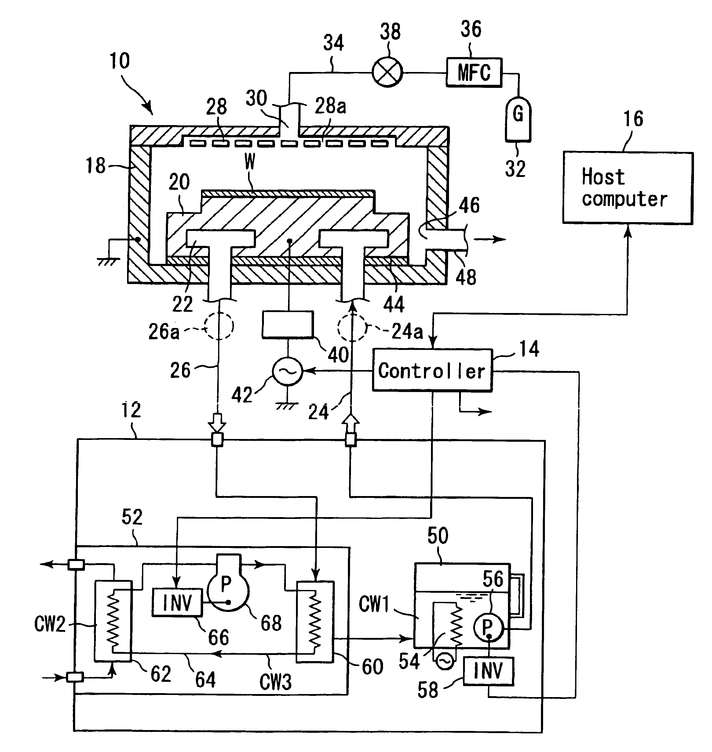
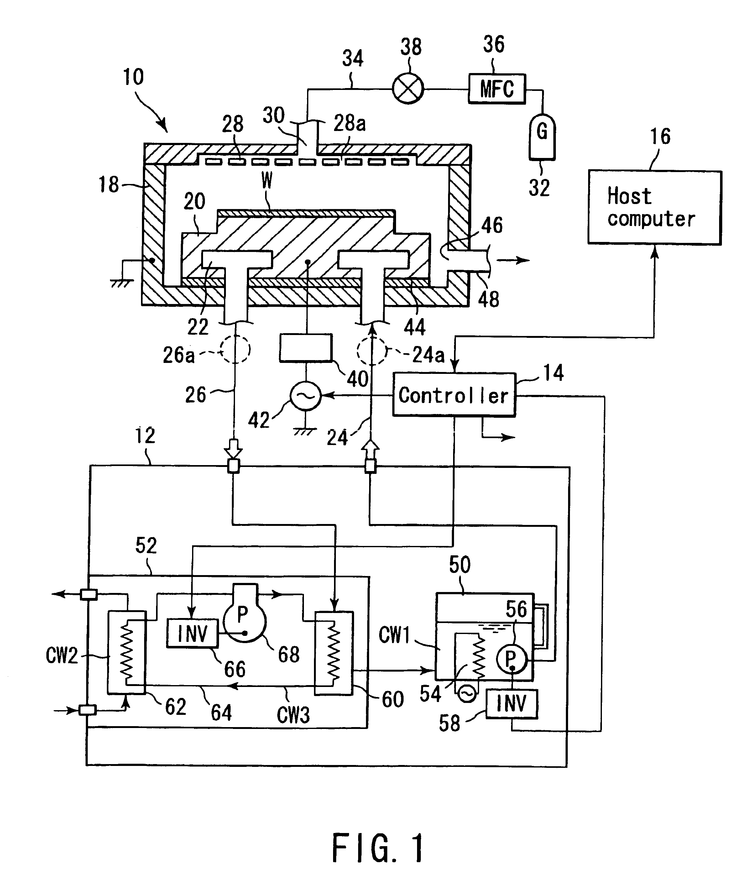
[0059]FIG. 1 is a view showing the structure of a semiconductor processing system according to a first embodiment of the present invention. This processing system includes a processing apparatus 10, a chiller unit 12, a controller 14, and a host computer 16.
[0060]For example, the processing apparatus 10 is structured as a plasma etching apparatus, and has a process chamber 18, which can be airtightly closed. A lower electrode 20 is disposed at the center of the process chamber 18, and functions also as a worktable (susceptor) for placing a substrate (e.g., a semi-conductor wafer) W thereon.
[0061]For example, the lower electrode 20 is formed of an aluminum plate block. The plate block is provided with a cooling medium room 22 formed therein, which, e.g., annularly extends in the angular direction. The cooling medium room 22 is connected to a cooling medium supply line 24 and cooling medium collection line 26 to form a cooling medium circulation passage. As described...
second embodiment
[Second Embodiment]
[0101]FIGS. 4 and 5 show a substrate processing device according to a second embodiment of the present invention. This substrate processing device has two cassette chambers 111 and 112 of airtight structure, into which are transferred cassettes (substrate transfer containers) C, which store multiple wafers, which are the substrates. These cassette chambers 111 and 112 are arranged aligned in a horizontal row, and therefore the cassettes C that are placed in them are aligned on a straight line to the left and right of each other. Cassette chambers 111 and 112 correspond to, respectively, the first substrate transfer container chamber, which forms the first placement area, and the second substrate transfer container chamber, which forms the second placement area.
[0102]Cassette chambers 111 and 112 each have a gate door GD on the atmosphere side, and the space with the atmosphere is airtightly partitioned by this gate door GD. Provided inside cassette chambers 111 an...
third embodiment
[Third Embodiment]
[0133]FIGS. 13 and 14 show a substrate processing device according to a third embodiment of present invention. This substrate processing device has, for example, two cassette chambers 211 and 212 of airtight structure, into which are transferred cassettes (transfer containers) C, which store multiple wafers, which are the substrates. Cassette chambers 211 and 212 each have a gate door GD on the atmosphere side, and the space with the atmosphere is airtightly partitioned by this gate door GD. Provided inside cassette chambers 211 and 212, as shown in FIG. 14, is elevator part 211b for raising and lowering cassette placement platform 211a and successively positioning the wafer retention grooves inside cassette C to the access level of the first transfer device, which is discussed below.
[0134]First transfer chamber 213, which is of airtight structure, is airtightly connected to the interior side of cassette chambers 211 and 212, and second transfer chamber 216, which ...
PUM
 Abstract
Description
Claims
Application Information


