Active matrix organic electro luminescence device panel

a luminescence device and active matrix technology, applied in the field of organic electro luminescence devices, can solve the problems of limiting the overall compactness of the panel, the entire mounting of the peripheral circuit of the panel, etc., and achieve the effect of increasing circuit integration

Active Publication Date: 2006-01-24
LG DISPLAY CO LTD
View PDF2 Cites 18 Cited by
  • Summary
  • Abstract
  • Description
  • Claims
  • Application Information

AI Technical Summary

Benefits of technology

[0015]An object of the present invention is to provide an active matrix organic electro luminescence device panel which increases circuit integration and provides a compact AMOLED panel.

Problems solved by technology

Accordingly, the related-art AMOLED panel structure has a disadvantage in that the peripheral circuit of the panel is entirely mounted on the PCB.
As a result, a wire structure of the first substrate is also complicated, thereby limiting the overall compactness of the panel.

Method used


Image

  • Active matrix organic electro luminescence device panel
  • Active matrix organic electro luminescence device panel
  • Active matrix organic electro luminescence device panel

Examples


Embodiment Construction

[0029]Reference will now be made in detail to the preferred embodiments of the present invention, examples of which are illustrated in the accompanying drawings. Wherever possible, the same reference numbers will be used throughout the drawings to refer to the same or like parts.

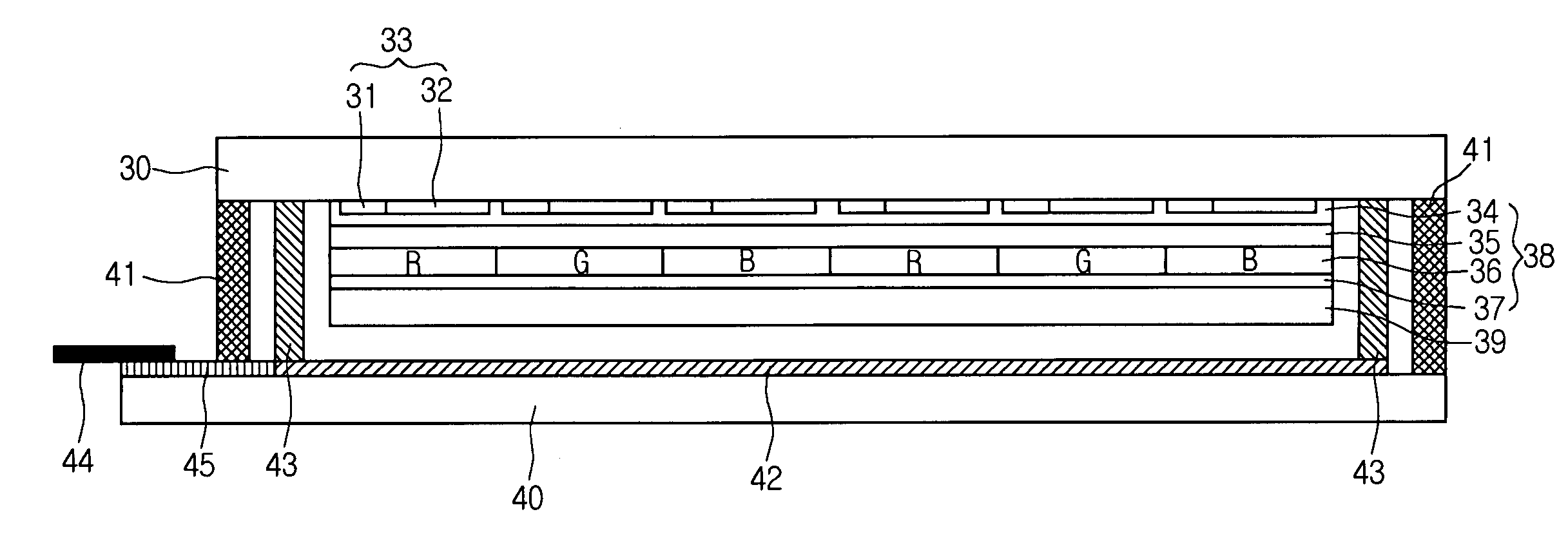
[0030]FIG. 3 is a sectional view illustrating an AMOLED panel according to the present invention. Referring to FIG. 3, the AMOLED panel includes a plurality of thin film transistors 31 and a plurality of first electrodes (pixel electrodes) 32, which are respectively in pixels 33 arrayed in matrix. Here, the pixels 33 are respectively formed in regions, which are defined between a plurality of gate lines (not shown) and a plurality of data lines (not shown). Further, an organic electro luminescence layer 38 and a second electrode (cathode) 39 are sequentially formed on the pixel electrodes 32.

[0031]More particularly, the organic electro luminescence layer 38 includes a hole injection layer (HIL) 34, a hole tr...


PUM


Abstract

An active matrix organic electro luminescence device panel includes: a first substrate having a plurality of thin film transistors and a plurality of first electrodes that define regions arrayed in matrix that each contain a pixel, wherein each pixel has an organic electro luminescence layer and a second electrode, which are sequentially formed on one of the first electrodes; a second substrate being positioned over the second electrode to prevent the organic electro luminescence layer from being degraded due to oxygen and moisture; and a sealant that adheres the first and second substrates to each other, wherein a plurality of wires and a driver are formed on the second substrate to provide a signal for driving the first electrodes.

Description

[0001]This application claims the benefit of Korean Patent Application No. 42407 / 2003 filed in Korea on Jun. 27, 2003, which is hereby incorporated by reference.BACKGROUND OF THE INVENTION[0002]1. Field of the Invention[0003]The present invention relates to an organic electro luminescence device, and more particularly, to an active matrix organic electro luminescence device panel in which a peripheral circuit is integrated and mounted on a second substrate not having a pixel.[0004]2. Description of the Related Art[0005]Cathode Ray Tube (CRT) display devices and liquid crystal display (LCD) devices are the most commonly used display devices. However, as a flat panel display devices are increasingly required to occupy smaller spaces, be lighter in weight and / or have a larger display size, an organic electro luminescence device (hereinafter, referred to as “organic EL device”) is being rapidly developed as a viable flat panel display device. Several products have been delivered to a ma...

Claims


Application Information

Patent Timeline
Patent Type & Authority Patents(United States)
IPC IPC(8): H01L31/0392H01L29/04H01L31/036H01L31/0376H01L31/20H05B33/22H01L27/32H01L51/52
CPCH01L51/524H01L27/3276H10K59/131H10K50/841H05B33/22
Inventor PARK, JAE YONGPARK, JOON KYU
Owner LG DISPLAY CO LTD
Why Eureka
Try Eureka