Driving of data lines used in unit circuit control

a technology of unit circuits and data lines, applied in static indicating devices, instruments, solid-state devices, etc., can solve the problems of difficult to construct a large display panel using, considerable time required to drive data lines, etc., and achieve the effect of shortening the driving time of data lines

Active Publication Date: 2006-01-24
ELEMENT CAPITAL COMMERCIAL CO PTE LTD
View PDF16 Cites 104 Cited by
  • Summary
  • Abstract
  • Description
  • Claims
  • Application Information

AI Technical Summary

Benefits of technology

[0008]Accordingly, an object of the present invention to shorten the driving time of data lines used in unit circuits.

Problems solved by technology

When the electrostatic capacitance Cd of the data lines is large, considerable time is required to drive the data lines.
It has been very difficult to construct a large display panel using organic EL elements because the large number of organic EL elements require very high driving speed.
The above mentioned problem is not limited to display devices using organic EL elements, but is also common to display devices and electro-optical devices using current-driven light-emitting elements other than organic EL elements.
Furthermore, this problem is not limited to light-emitting elements, but is also common to general electronic devices using current-driven elements that are driven by an electric current.

Method used


Image

  • Driving of data lines used in unit circuit control
  • Driving of data lines used in unit circuit control
  • Driving of data lines used in unit circuit control

Examples


second embodiment (

B. Second Embodiment (Current Addition 2)

[0093]FIG. 10 is a block diagram which shows the schematic structure of a display device as a second embodiment of the present invention. This display device differs from the first embodiment in that a data line driver 400a is installed on the side of the power supply voltage Vdd. Furthermore, as will be described below, the internal structure of the single-line drivers 410a and the internal structure of the pixel circuits 210 also differ from those of the first embodiment.

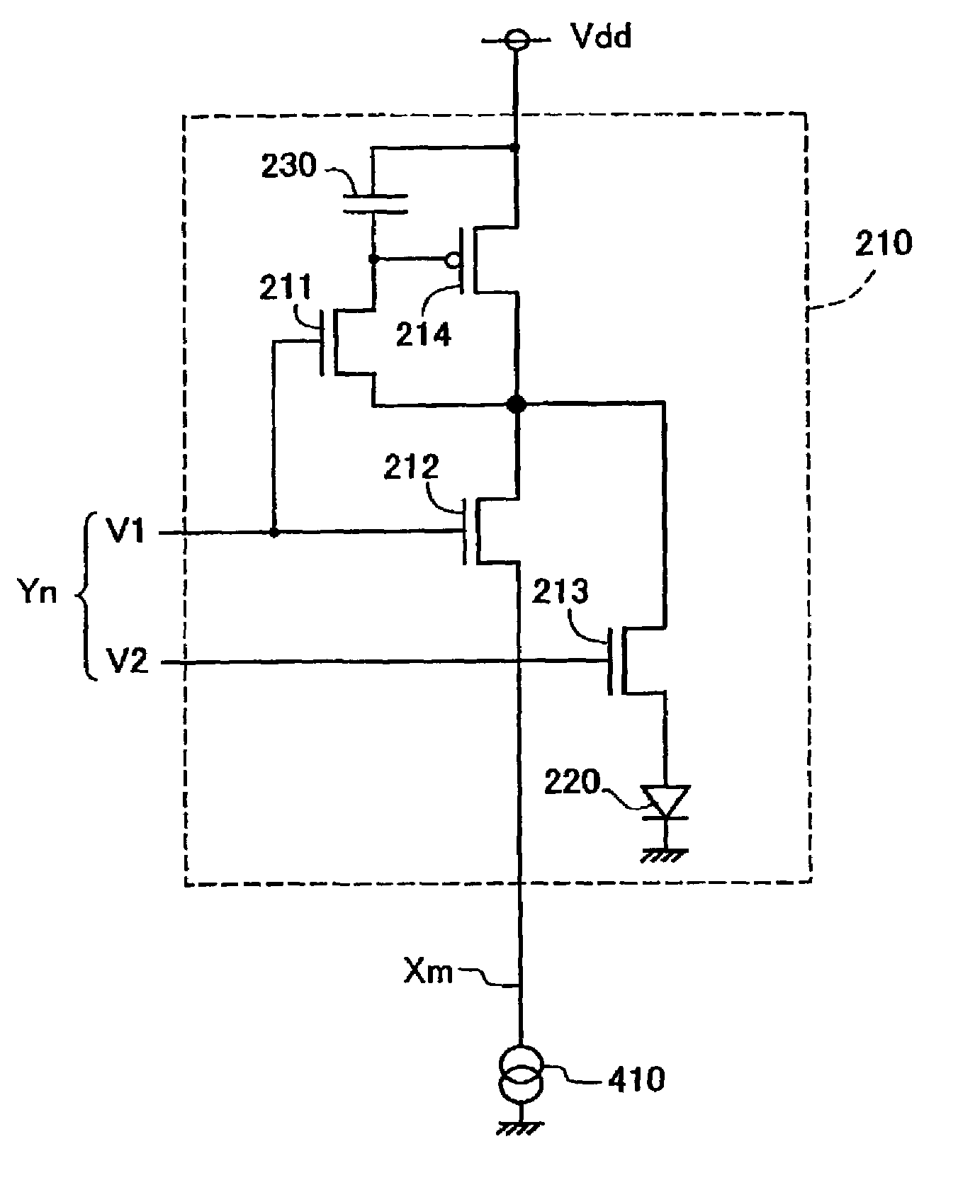
[0094]FIG. 11 is a circuit diagram which shows the internal structure of one pixel circuit 210a. This pixel circuit 210a is a so-called Sarnoff type current-programmable circuit. This pixel circuit 210a has an organic EL element 220, four transistors 241 through 244, and a storage capacitor 230. Furthermore, the four transistors are p-channel type FETs.

[0095]The first transistor 241, storage capacitor 230 and second transistor 242 are connected in series in this order to th...

third embodiment (

C. Third Embodiment (Current Addition 3)

[0103]FIG. 16 is a circuit diagram that shows one of the single-line driver circuits 410b in a third embodiment of the present invention. The data signal generating circuit 420 inside this single-line driver 410b is the same as that of the first embodiment shown in FIG. 6; however, the structure of the additional current generation circuit 430b differs from that of the first embodiment. Specifically, this additional current generation circuit 430b has two sets of series connections of a switching transistor 43 and driving transistor 42, and these series connections are connected in parallel with each other. For example, the ratio of the gain coefficients βc of the two driving transistors 44 is set at 1:2. The additional current control signal Dp is a two-bit signal in this embodiment. In cases where this additional current generation circuit 430b is used, the additional current value Ip can be arbitrarily set at any of four levels correspondin...

fourth embodiment (

E. Fourth Embodiment (Pre-Charging)

[0110]FIG. 18 is a block diagram which illustrates the structure of a display device as a fourth embodiment of the present invention. In this display device, a pre-charging circuit 600 is installed for each of the data lines Xm (m=1 through M) of the display device of the first embodiment shown in FIG. 3. The remaining structure is the same as that shown in FIG. 3. However, the electrostatic capacitance Cd of the data lines is omitted for the sake of convenience of illustration. Furthermore, circuitry that does not have an additional current generation circuit 430 (FIG. 6) may be used as the single-line drivers 410.

[0111]Pre-charging circuits 600 are respectively connected to each data line Xm in a position between the display matrix section 200 and the data line driver 400. These pre-charging circuits 600 are each constructed from a series connection of a pre-charging power supply Vp which is a constant voltage source, and a switching transistor 6...


PUM


Abstract

The display matrix section 200 has pixel circuits 210 arranged in the form of a matrix, a plurality of gate lines Y1, Y2 . . . that extend in the row direction, and a plurality of data lines X1, X2 . . . that extend in the column direction. The scan lines are connected to a gate driver 300, and the data lines are connected to a data line driver 400. A pre-charging circuit 600 or additional current generation circuit is installed for each data line as means for accelerating the charging or discharging of the data line. For each data line, charging or discharging is accelerated by pre-charging or current addition prior to the completion of the setting of the light emission level in the corresponding pixel circuit 210.

Description

BACKGROUND OF THE INVENTION[0001]1. Field of the Invention[0002]The present invention relates to a technique for driving data lines used in control of unit circuits, such as pixel circuits of a display device.[0003]2. Description of the Related Art[0004]In recent years, electro-optical devices using organic EL elements (organic electroluminescent elements) have been under development. Organic EL elements emit light themselves, and do not require back lighting. Accordingly, it is expected that such elements will make it possible to achieve display devices that have a lower power consumption, high visual field angle and high contrast ratio. Furthermore, in the present specification, the term “electro-optical device” refers to a device that converts an electrical signal into light. A typical example of an electro-optical device is a device that converts an electrical signal expressing an image into light representing an image; such a device is especially suitable as a display device.[0...

Claims


Application Information

Patent Timeline
Patent Type & Authority Patents(United States)
IPC IPC(8): G09G5/00G09G3/30G09G3/20G09G3/32G09G3/36H01L51/50
CPCG09G3/325G09G3/3275G09G3/3283G09G2320/0223G09G2300/0861G09G2310/0248G09G2310/027G09G2300/0842G09G3/30
Inventor KASAI, TOSHIYUKI
Owner ELEMENT CAPITAL COMMERCIAL CO PTE LTD
Why Eureka
Try Eureka