
Multi-port memory architecture

a multi-port memory and architecture technology, applied in information storage, static storage, digital storage, etc., can solve the problems of noise rendering simultaneous read and write operations difficult or potentially impossible, difficult or impossible to accurately sense the data bit being read, etc., to achieve accurate discrimination and low noise

Active Publication Date: 2006-01-24
TWITTER INC
View PDF5 Cites 31 Cited by
  • Summary
  • Abstract
  • Description
  • Claims
  • Application Information

AI Technical Summary

Benefits of technology

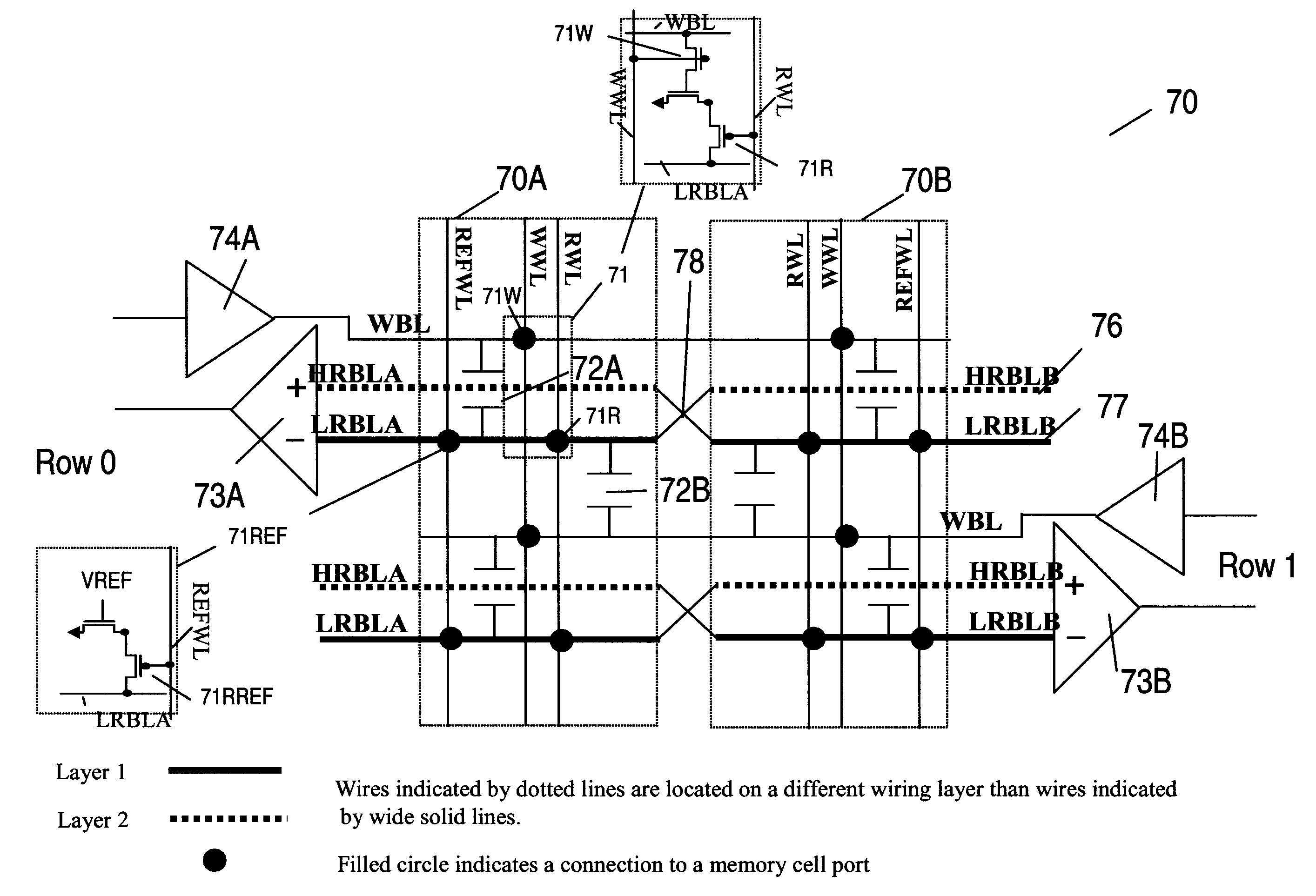
[0014]It is another object of the invention to provide a method and a memory configuration that overcomes read bitline sensing problems in a multi-port memory device due to adjacent write bitline to the read bitline coupling noise during concurrent read and write operations.
[0017]The invention describes an open read bitline configuration as well as a re-entrant read bitline configuration and a re-entrant write bitline configuration. Each is effective in providing a dense, low noise simultaneous read-write array.

Problems solved by technology

When WBL changes voltage, the coupling capacitance between WBL and the nearby RBL causes a voltage disturbance on RBL.
This noise on RBL makes it difficult or impossible to accurately sense the data bit that is being read.
The coupling noise renders simultaneous read and write operations difficult or potentially impossible.
Shielding techniques eliminate the coupling noise, however, at the expense of a significantly increased cell area.
The coupling noise between WBL and RBL presents a unique problem that occurs during a simultaneous read and write operation.
Conventional BL twisting methods are not applicable to cancel the noise because of the single ended RBL and WBL configuration defining the dual-port cells.

Method used


Image

  • Multi-port memory architecture
  • Multi-port memory architecture
  • Multi-port memory architecture

Examples


Embodiment Construction

[0029]FIG. 6 shows a first embodiment of the present invention which utilizes an open bitline configuration for the read bitline (RBLA in the array 60A and RBLB in the array 60B). Memory 60 consists of two arrays 60A and 60B, each containing a plurality of 3T gain cells 61 arranged in a matrix formation. Practitioners in the art will realize that other memory cells having two general ports or separate read and write ports may be used to configure the memory array to enable simultaneous read and write operations. Each memory array 60A and 60B includes a reference wordline REFWL that is coupled to reference cells 61R, each coupling to the corresponding RBLs (RBLA in the array 60A and RBLB in the array 60B). Different configurations of the reference cells may be used. For simplicity, REFWL in the array 60A and RWL and WWL in the array 60B are not shown.

[0030]When reference cell 61R is accessed, RBL in the activated array discharges to a level or at a rate that is at half-way the value ...


PUM


Abstract

A multi-port memory architecture utilizing an open bitline configuration for the read bitline is described. The memory is sub-divided into two arrays (A and B) consisting of memory gain cells arranged in a matrix formation, the cells having two general ports or separate read and write ports to enable simultaneous a read and write operation. Each memory array includes a reference wordline coupled to reference cells. When the reference cell is accessed, the read bitline (RBL) discharges to a level at half the value taken by a cell storing a 0 or 1. Each pair of RBLB in the same column of the two arrays is coupled to a differential sense amplifier, and each write bitline (WBL) in the two arrays is linked to write drivers WBLs in the two arrays are driven to the same voltage and at the same slew rate. The WBL swing in each array creates coupling noise by the bitline-to-bitline capacitors. For a given sense amplifier and its associated RBLs, the coupling creates an identical coupling noise on RBLA and RBLB that are positioned in the two arrays A and B. This common mode noise is rejected by the differential sense amplifier. Thus, a read sense amplifier can accurately discriminate between the signal by activating the cell by way of RWL, and the reference cell by way of REFWL.

Description

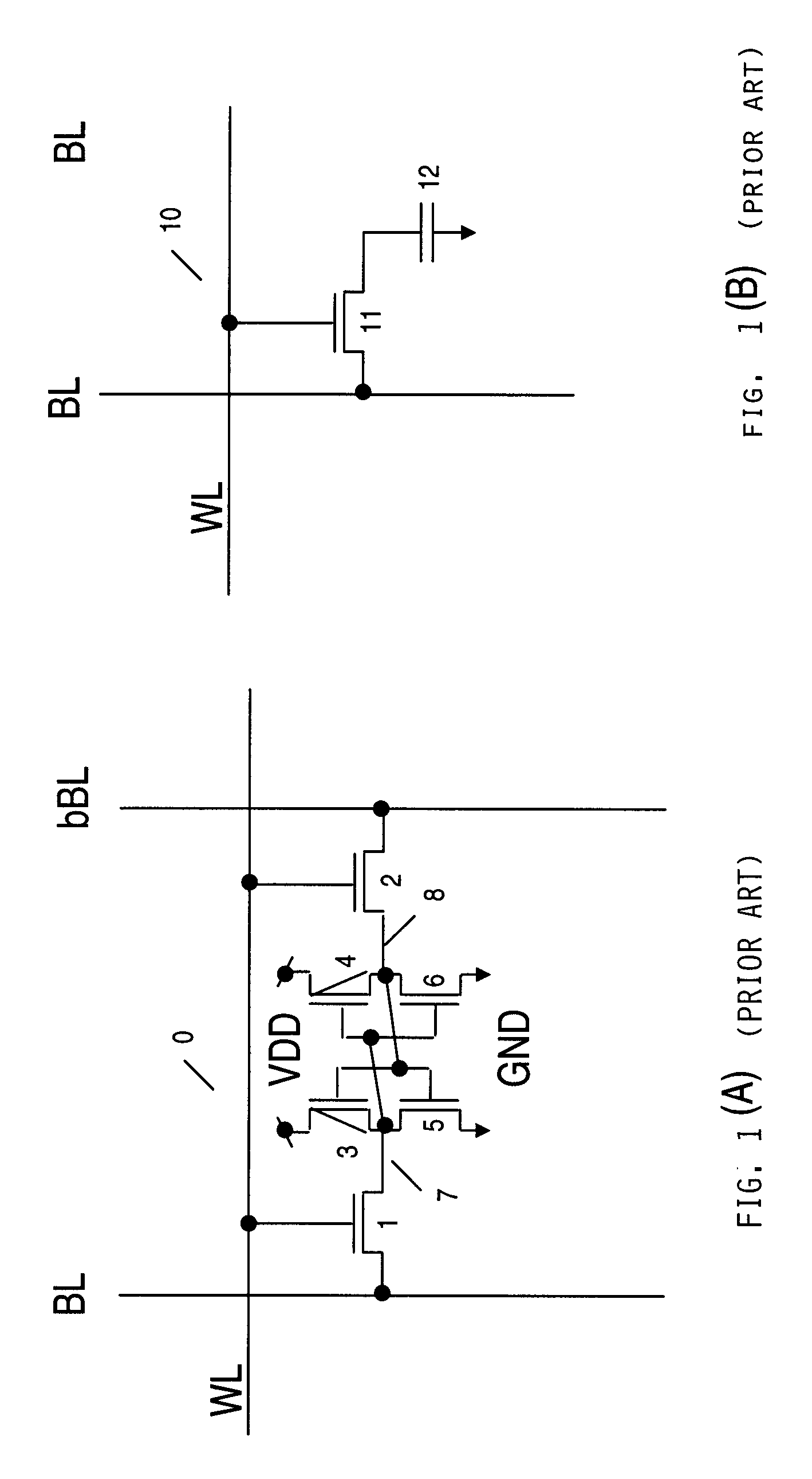
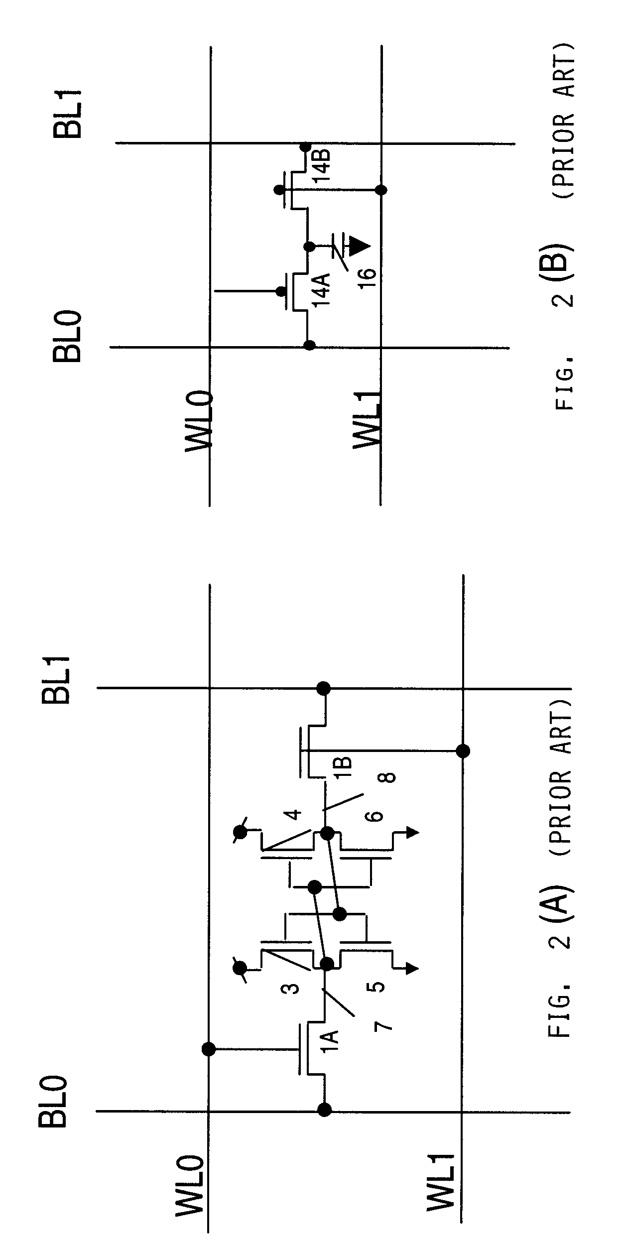
BACKGROUND OF INVENTION[0001]This invention describes the architecture of a multi-port memory, and more particularly, it describes a method and configuration to reduce the noise on read bitlines created during a simultaneous read and write operation in a multi-port memory.[0002]Single port memories allow either one read or one write operation during each cycle. Typically, a single port memory consists of either six transistor static memory cells (6T SRAM) or single transistor dynamic cells (1T).[0003]FIG. 1A shows a transistor level schematic of a typical 6T SRAM cell 0. It consists of four NMOS transistors 1, 2, 5, and 6, and two PMOS transistors 3 and 4. PMOS 3 and 4 and NMOS 5 and 6 transistors configure a CMOS cross-coupled latch, which maintains a data bit as a storage element. NMOS 1 and 2 couple nodes 7 and 8 to biltlines BL and bBL when a wordline WL is activated. This allows the data bit to be read to or written from bitlines BL and bBL.[0004]FIG. 1B depicts a transistor le...

Claims


Application Information

Patent Timeline
Patent Type & Authority Patents(United States)
IPC IPC(8): G11C7/00G11C5/00G11C8/16G11C11/405G11C11/4099
CPCG11C8/16G11C11/4099G11C11/405
Inventor KIRIHATA, TOSHIAKIKIM, HOKIWORDEMAN, MATTHEW
Owner TWITTER INC
Learn More