Semiconductor integrated circuit device having a common DRAM block accessed by a plurality of logic circuits

a technology of integrated circuits and logic circuits, which is applied in the direction of memory adressing/allocation/relocation, digital storage, instruments, etc., can solve the problems of increasing the difficulty of the inability to perform memory optimization in the entire system lsi properly, and the small size of each sram, etc., to achieve a high degree of integration of dram, reduce device area overhead, and reduce the effect of peripheral circuit overhead overhead

Active Publication Date: 2006-01-24
CETUS TECH INC
View PDF5 Cites 36 Cited by
  • Summary
  • Abstract
  • Description
  • Claims
  • Application Information

AI Technical Summary

Benefits of technology

[0013]In view of the above problems, an object of the present invention is to provide a semiconductor integrated circuit device in which a plurality of logic circuits share a DRAM block without causing any decrease in data processing capability.
[0015]In the inventive device, since the DRAM block is shared by the plurality of logic circuits, area overhead caused by the peripheral circuits of the memory is reduced, which, in addition to the high degree of integration of the DRAM, permits a further decrease in the device area. Furthermore, the access circuit makes access to the DRAM block by performing time division processing, while the operation clock for the DRAM block is set at a higher frequency than the operation clock for the logic circuits, so that data transfer efficiency equal to, or higher than, that of the conventional configuration is achieved, thereby realizing high data processing capability.
[0019]In the inventive device, since the DRAM block is shared by the plurality of logic circuits, area overhead caused by the peripheral circuits of the memory is reduced, which, in addition to the high degree of integration of the DRAM, permits a further decrease in the device area. Furthermore, the access circuit makes access to the DRAM block by performing time division processing, while the serial / parallel conversion circuits for converting the number of bits of data are interposed between the logic circuits and the DRAM block. It is thus possible to establish the desired number of I / O bits. In addition, the first and second serial / parallel conversion circuits have different conversion rates for converting the number of bits, so that different numbers of I / O bits can be established for the first and second logic circuits. As a result, the memory space of the DRAM block is used most efficiently, thereby allowing the data region to be flexibly allocated to the logic circuits.
[0020]According to the present invention, the device area is reduced further, data transfer efficiency equal to, or higher than, that of the conventional configuration is achieved, and high data processing capability is realized. Moreover, the memory space of the DRAM block is used most efficiently, thereby allowing the data region to be flexibly allocated to the logic circuits.

Problems solved by technology

However, the conventional device has the following problems.
However, since the capacity of each SRAM is small, even if the ratio of the total memories to the chip becomes too high, the designer of the system LSI is not likely to notice that.
Consequently, memory optimization in the entire system LSI is not necessarily performed properly in many cases.
As a result, while the ratio of embedded memories has been increasing, memory optimization in the entire system LSI has become more difficult.
Moreover, an SRAM, whose memory cells each consist of six transistors, is not suited for having a large capacity in terms of integration.
These problems have also presented difficulties in achieving the optimization of entire memories.

Method used


Image

  • Semiconductor integrated circuit device having a common DRAM block accessed by a plurality of logic circuits
  • Semiconductor integrated circuit device having a common DRAM block accessed by a plurality of logic circuits
  • Semiconductor integrated circuit device having a common DRAM block accessed by a plurality of logic circuits

Examples


Embodiment Construction

[0027]Hereinafter, preferred embodiments of the present invention will be described with reference to the accompanying drawings.

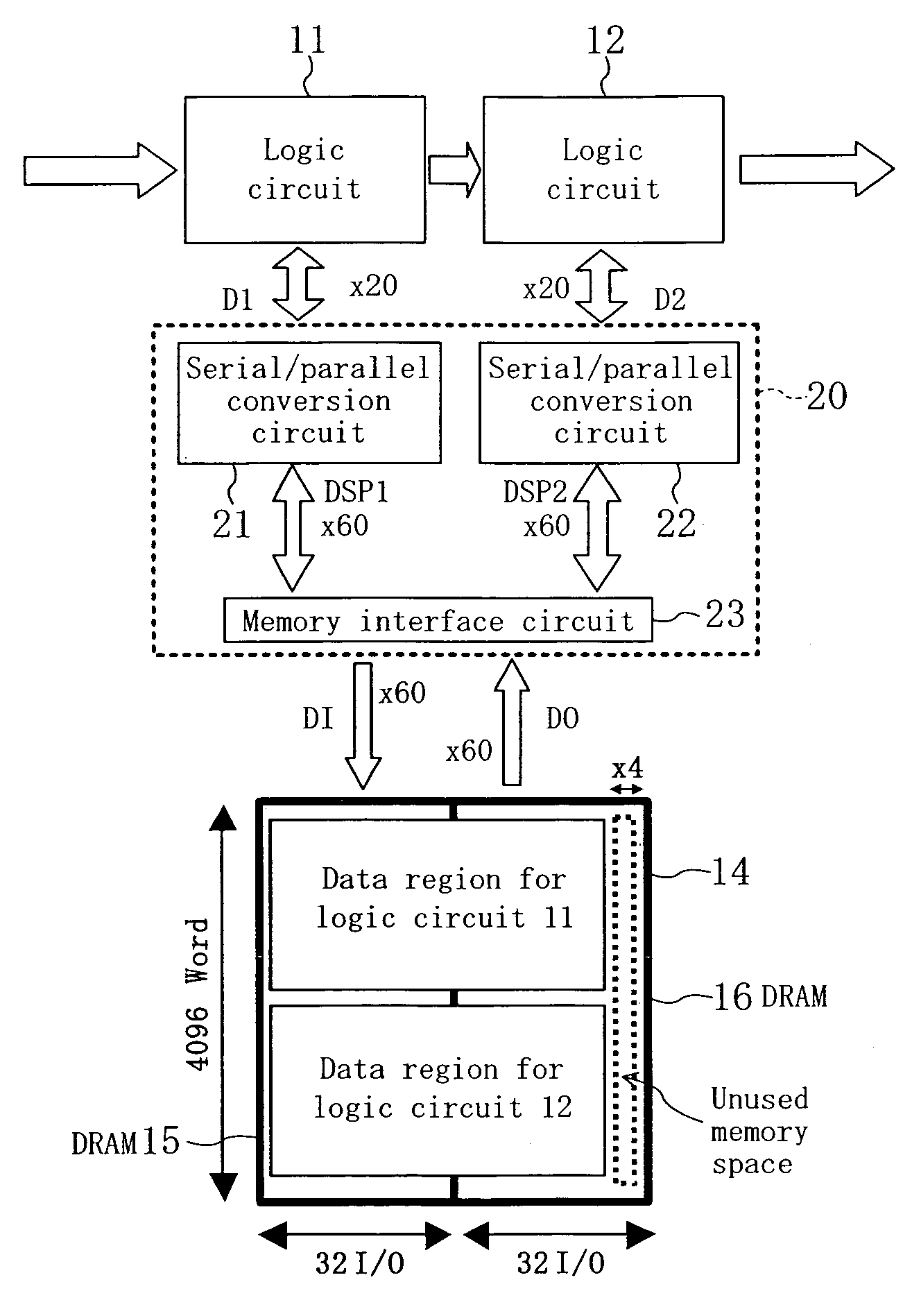
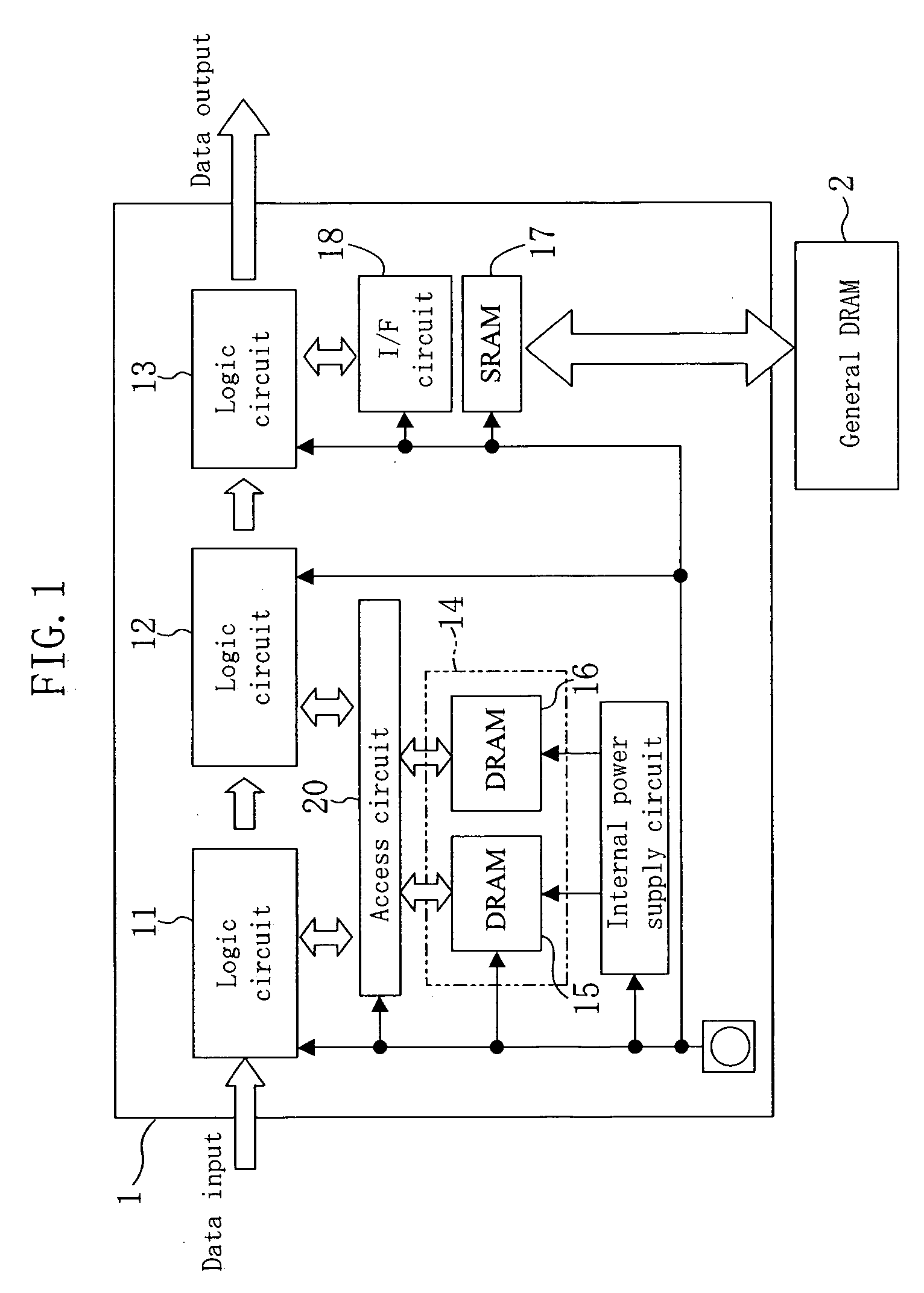
[0028]FIG. 1 is a block diagram illustrating the main components of a semiconductor integrated circuit device in accordance with an embodiment of the present invention. In FIG. 1, the semiconductor integrated circuit device 1 includes a plurality of logic circuits 11, 12, and 13 for realizing respective predetermined processing functions, a DRAM block 14 including two DRAMs 15 and 16, and an SRAM block 17. The DRAM block 14 is accessible from the logic circuits 11 and 12 via an access circuit 20, while the SRAM block 17 is accessible from the logic circuit 13 via an I / F circuit 18. The access circuit 20 is designed so as to be capable of performing time division processing so that the logic circuits 11 and 12 can share the DRAM block 14. The SRAM block 17 is configured capable of transferring data to / from a general DRAM 2.

[0029]FIG. 2 illustrates an exempla...


PUM


Abstract

A plurality of logic circuits access a DRAM block by way of an access circuit. The operation clock for the DRAM block is set at a higher frequency than the system clock for the logic circuits. Outputs of a first bit width from the logic circuits are subjected to serial / parallel conversion into data of a second bit width and the data is written into the DRAM block.

Description

CROSS-REFERENCE TO RELATED APPLICATION[0001]The disclosure of Japanese Patent Application No. 2004-071227 filed on Mar. 12, 2004 including specification, drawings and claims is incorporated herein by reference in its entirety.BACKGROUND OF THE INVENTION[0002]The present invention relates to a semiconductor integrated circuit device in which a plurality of logic circuits and a common DRAM block accessed by those logic circuits are incorporated.[0003]Conventionally, memories corresponding to individual logic circuit blocks have been embedded on a system LSI to achieve performance improvement and power consumption reduction. FIG. 6 is a block diagram illustrating an example of a conventional semiconductor integrated circuit device. As shown in FIG. 6, a static random access memory (which will be hereinafter referred to as an “SRAM”) 51 having a size ranging from about several kilobits to about several hundred kilobits is used as a storage section for data which is required to be proces...

Claims


Application Information

Patent Timeline
Patent Type & Authority Patents(United States)
IPC IPC(8): G11C8/18G06F12/00G06F12/04G11C7/00G11C8/00G11C11/4063
CPCG11C7/10G11C7/1006G11C2207/107G11C11/40
Inventor KURODA, NAOKINAKAI, YUJI
Owner CETUS TECH INC
Why Eureka
Try Eureka